There are a lot of ways to build quick prototypes. These days it’s even arguable that you should have a PCB made since you can get them so cheaply and quickly… and then also, if you go on to make a production grade project you’re further along.
However, I decided to do something really old school and just put the parts into a perf board. This is actually a pretty rare way of doing things these days since I won’t be using any kind of purpose built prototyping PCB, nor manhattan style construction, nor any of the other popular methods. I’m not even going to use perf board pins (that’s another old-school method… can you even buy those anymore??)
Instead, I’ll plan it out so that only the component leads and a bit of wire are required. With a bit of practice this method is perfectly fine for anything that’s not going to be using RF (because there is no ground plane of any kind with this method). This method is just shy of being sculpture… but working this way is quick because it doesn’t require anything more than what you have on hand, and therapeutic because getting it all together is a bit of an art form: working with your hands, bending wires just right, growing the circuit somewhat organically one part at a time… limited only by the parts themselves, your patience, and your imagination.
Plan the layout.
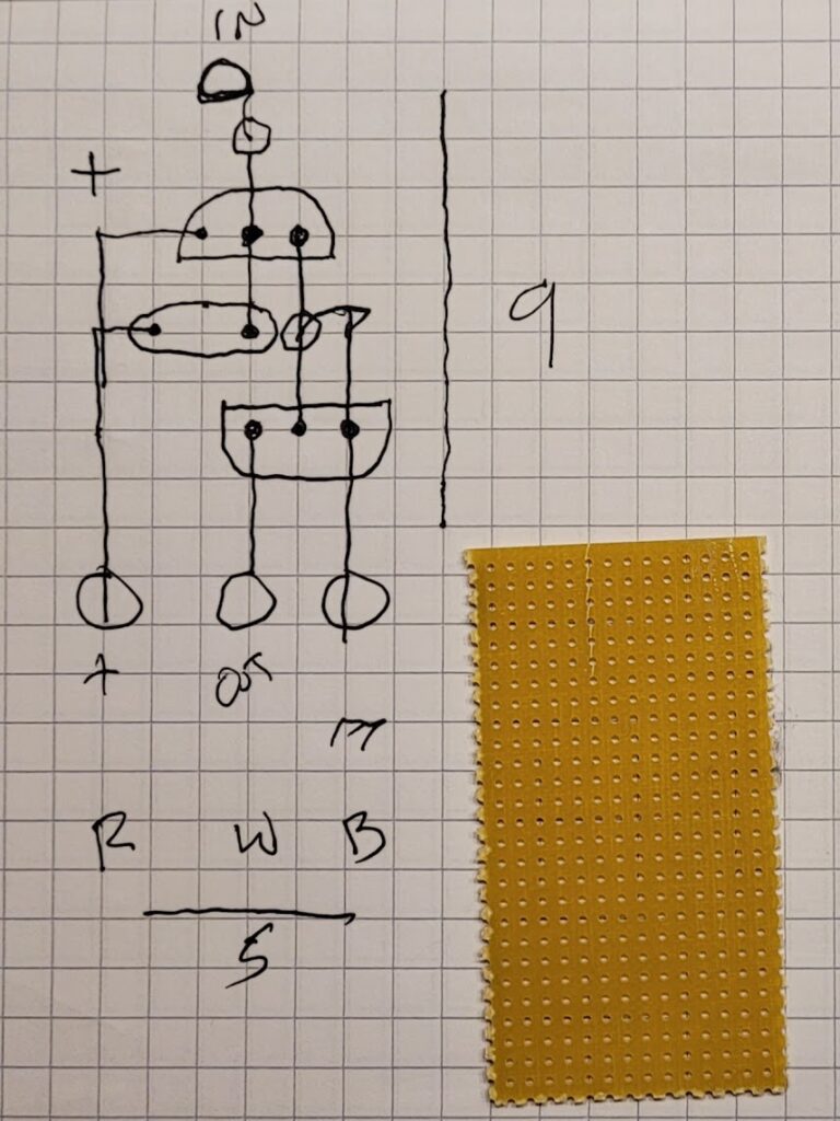
Lay a piece of perf board on a piece of graph paper, and imagine that each crossing point is a hole in the perf board. I like to work from the top side with an “x-ray” view of the wiring. Actually, the wiring might be on either side so “x-ray” means you can see it no matter where it is.
This approach will limit you to making circuits that don’t require jumpers (mostly)… and that tends to keep things simple. It’s not that you can’t use a jumper if you wish; but it’s easier if you avoid them… and that will make you think a little more carefully as you proceed.
You’ll also want to be very careful about the pin-outs of any components you’re using. Check everything more than twice as you lay out the circuit. It sometimes helps to actually pick up the part, find the correct pins, and put it in the perf board somewhere just so you can see and feel how that goes together. Not everyone can do all of that in their head (I can, but I have had a lot of practice). Seeing your drawing right next to an actual part in a board can be a very powerful way of making it all “real” so that you can reason about it without too much effort. The more time you spend relating the two physically the easier it will be (eventually) for you to see that process in your mind’s eye.
Generally proceed from input to output; complete the nets for any given component before moving on to the next (but have in mind where the next connected parts will fit into the layout); and try to keep the rails on the outside edges of the board. By working this way, eventually you will complete all of the work for one section of your design before moving on to the next section. As you complete each section it’s a good time to check that it’s really complete and everything is properly connected before moving on to the next.
Don’t be afraid to start over if you run into a dead-end of some kind… like painting yourself into a corner in a room, it’s possible to go through this process and eventually find out that you don’t have room for something; or maybe you might discover a better layout along the way. At this point it’s only paper! Toss it out and start again… this time starting from experience… it will go faster and be better each time you iterate through this process (if you need to).
After having done this for a while, I can usually get through a complete design in a single pass with almost no re-work… mostly because at this point I can see forward several steps at each stage and because I can have a rough block-diagram kind of model in mind even before I begin. All of that comes with experience and it’s the kind of thing that can save you huge amounts of time and trouble if and when you do start designing PCBs… starting with a “rats nest” and dragging parts into place, of course (you don’t use auto-routing do you!!!).
In this case, I started with the input (one resistor, yeah, not much of a section), then since it’s next connection is to the input amplifier I completed that next: first by placing the input transistor so that it’s base is right next to it’s side of the input resistor, then by adding the filter capacitor from that net to the emitter side of the transistor and the positive rail, then I cheated just a little by adding in the pull down resistor that’s at the gate of the output stage… I say I cheated but I didn’t really, it was a natural progression to the next stage and (depending on how you look at it) the collector resistor of the input amplifier IS the pull-down resistor for the gate of the output switch… either way, that part completes the input section and makes for a good time to look it over and check that all of the circuit up to that point is complete and will work as expected. A pause, then on to adding in the FET, and so forth…
I like to imagine actually mounting the parts as I draw them on the page so that when it comes time for physically mounting the parts and soldering them together I’ve already had a dry-run through that process.
This includes considering how the parts will hold each other in place through that process and when the project is completed. Some combination of bent wires against the circuit board, little loops, and other mechanical tricks will be combined to make this process work. Working out those details while laying out the design drawing is a powerful way to avoid problems during assembly and after things are complete.
By the time you’ve finished the drawing you should have complete confidence that all of the nets have been accounted for and that the physical rendering of the circuit will not only work, but might even have some aesthetic value 😉
Cut out some perf board.
Once you’ve finished your drawing you will know precisely how many “holes” of your perf board are required by counting the squares on the graph paper that are taken up by the completed design. Use a marker (sharpie) to sketch out the boundaries on your perf board and then score over those with an exacto knife. After that, you should be able to fairly easily use needle nose pliers to cleanly break the perf board along those lines.
I like to use the long edge of the pliers along a scored line and start bending the board at one end of it… that usually leads to a nice clean break as the needle nose pliers will tend to protect the part of the board that they cover.
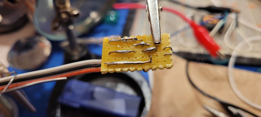
Mount the input resistor.
Right away I start with some of those little physical tricks I mentioned. One end of the input resistor must also create a terminal for connecting the input. Here, I’ve used that to physically hold the resistor in place when it’s first mounted.
Using the end-on style of mounting this resistor (as was popular in old transistor radios) I chose to put the body of the resistor close to the input transistor. This way, the other lead of the resistor makes a handy test point and also is easier to work with while weaving the end of it through the perf board and back to make an input terminal (loop). Down through one hole, up around the edge of the board and back down through an adjacent hole bent into a loop. This lead holds the input resistor into the board early and acts as a strain relief for any wire(s) that might be soldered to the terminal later.
Mount the input transistor.
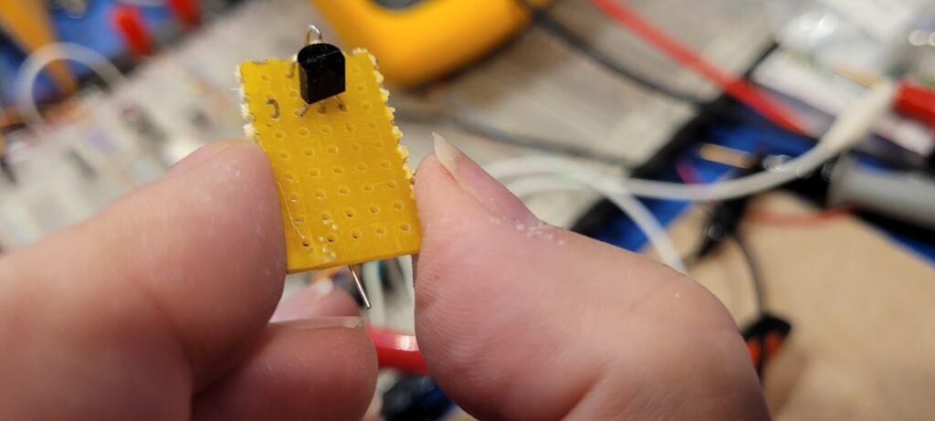
Next up I added the input transistor. This being a PNP transistor, I know I want the emitter toward the positive rail (eventually), and the collector toward the negative (ground) rail. Luckily the pin out has the base in the middle so it’s really easy to get precisely what I want just by making sure the flat side is away from the input resistor and the input resistor is “in the middle.”
To hold the transistor in place I can start by slightly splaying the leads out on the underside of the board, or perhaps even bending some of them into their final direction prior to soldering.
If you look closely you’ll see another physical trick similar to what was done with the input resistor. In this case, the emitter lead is weaved through the perf board to stick up through the top side eventually to connect to the positive rail and the filter capacitor. This required a little thinking ahead and was only one of several options; but I decided it was a good way to hold the transistor in place and provide options for binding the positive rail later.
Input connections underside.
Looking at the underside you can see that the input resistor lead is bent flat against the perf board and runs right next to the base lead of the input transistor. This way, the base lead can be laid flat right next to it in the other direction making for a tidy connection and a strong physical mount for both.
You can also see off to the right of that where the emitter lead has been fed back up through the perf board to connect to the positive rail and the filter capacitor (coming up next).
Add the filter capacitor.
Back on the topside of the board you can see how the filter capacitor fits perfectly (skipping a hole) between the extended emitter lead and the base lead. Here again was an opportunity during the planning stage to put a part through the perf board and understand exactly what size it is.
With the filter capacitor in place the emitter lead is bent down to meet it at the hole on that side. I actually tried to get the lead to go down through the same hole– but it was a bit too short and thick for that. No matter, I planned ahead so there will be plenty of ways to sure up this connection electrically.
Solder in place on the top side.
To start with, I just soldered the emitter lead to the filter cap lead on the top of the board. That works fine for these first steps and holds the filter capacitor in place while working on it’s other lead.
Connect filter capacitor to input, underside.
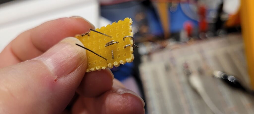
Back on the underside of the board the filter capacitor lead gets bent flat across the base lead and the input resistor lead. Having all three of these laying in parallel to each other will make for a good electrical connection.
Solder in place, underside.
Once soldered, the net for the base of the input amplifier is complete; and the net for the emitter side of the input amplifier is well prepped. Assembly of the circuit is progressing essentially in the same order as it’s planning was done.
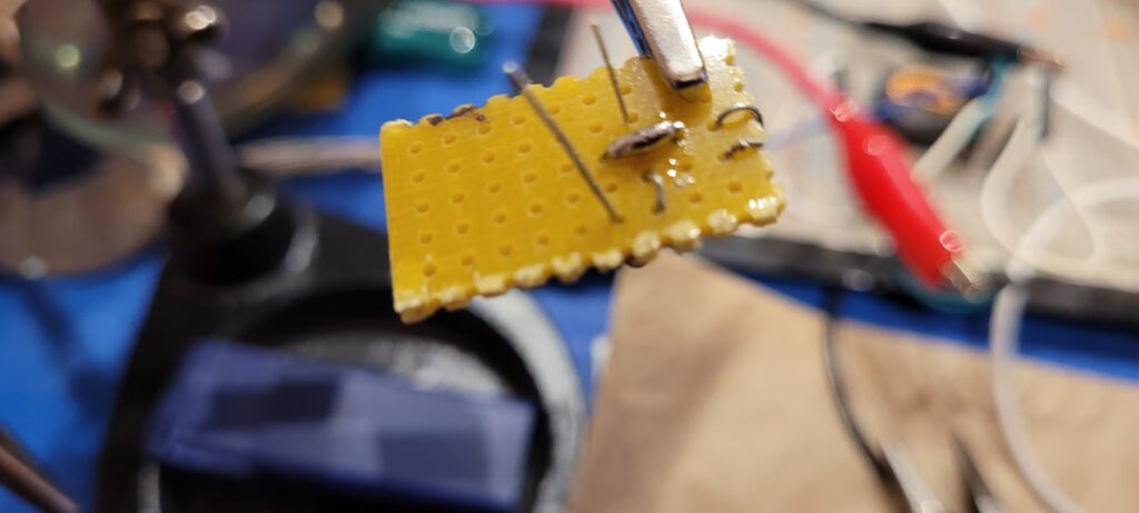
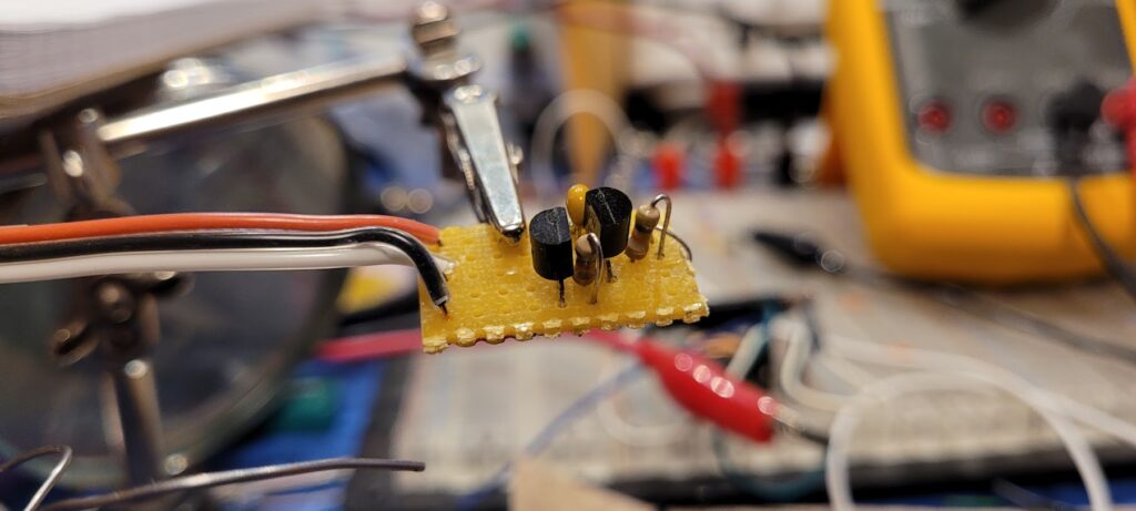
The output section is highly dependent on the power rails being in place so I decided to get that work done before installing the FET and other components. This kind-of breaks the rule of progressing from input to output… but not really since in this case best way to install the next section would be to have the power rails (the ground rail especially) in place first.
Wire for rails and output.
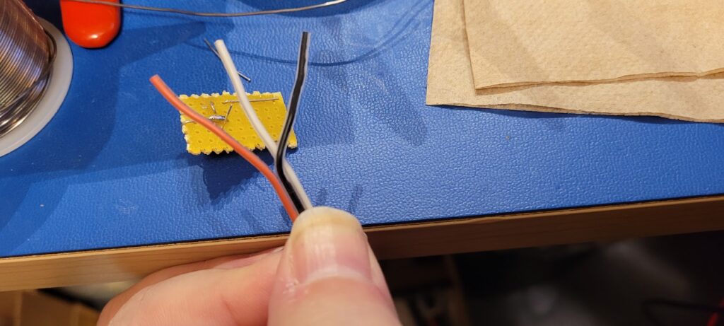
I happened to know I had some color coded ribbon wire when I started this so I planned to use it from the beginning. It normally has 4 conductors, but at this point I’d stripped off the green wire leaving a convenient red, black, and white. In other parts of the project the input is generally white so that works out perfectly.
The imperfect part is that the white is not in the middle– but it will be on the perf board… and as it turns out, with a little planning, even that won’t matter for long because I’ll be removing the white wire to create a terminal instead during integration. For now, however, having these all together in a ribbon will help hold things in place.
Wire for rails and output fed into board.
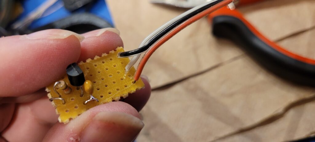
After stripping off sufficient insulation to reach back to the existing circuitry I put the wires through the perf board and bent their leads flat along the required straight lines on the underside.
Route the positive rail into place, underside.
The most useful next step is to complete the positive rail. Note that the wire ends up parallel to the lead from the filter capacitor; but it runs past that so that it can be fed into the hole where the emitter lead was previously woven back up through the board.
Positive rail soldered into place, underside.
Having soldered the positive rail to the filter capacitor lead, which was laid down parallel to it, and having extended that further to the emitter lead, the positive rail net is now complete and quite solid.
Reheat the emitter at the positive rail.
For good measure I reheated the emitter, filter capacitor, and positive rail on the topside of the board.
Add pull-down resistor to collector.
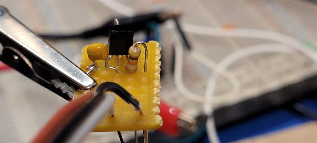
The next best connection to complete the input section and begin the output section is the pull-down resistor. Here you can see it mounted with it’s body at the collector of the input transistor and it’s tail going through the board in line with the negative rail.
In this case I opted to have the tail connect to ground since that is a safer thing to expose and also because it keeps the lead connected to the signal in the circuit as short as possible.
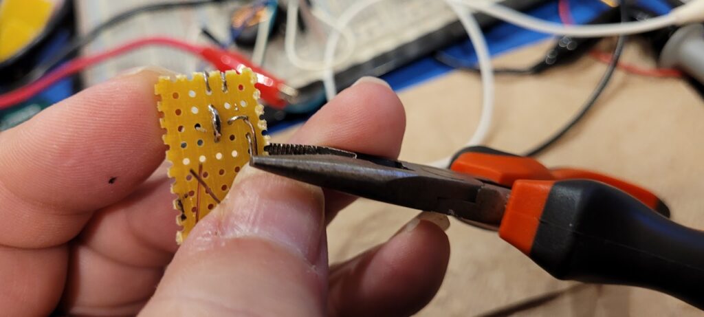
Bend pull-down resistor leads for ground rail and collector net.
Back on the underside, the tail of the pull-down resistor is extended along the path of the negative rail; and the body side lead is folded flat in parallel with the collector lead of the input transistor. The transistor lead is then extended along that path to eventually meet up with the gate of the output FET.
Solder collector lead.
With the collector lead soldered to the pull-down resistor the resistor is held solidly in place and it’s time to mount the output switch (FET).
Mount FET.
The pin-out of the FET is also convenient. In this case we can put the source in line with the ground rail, put the gate in the next hole in line with the collector of the input transistor, and end up with the open drain perfectly in line with the output wire. To do this, the flat side of the FET must face the flat side of the PNP transistor… but that conveniently makes for a nice space where the pull-down resistor can live comfortably.
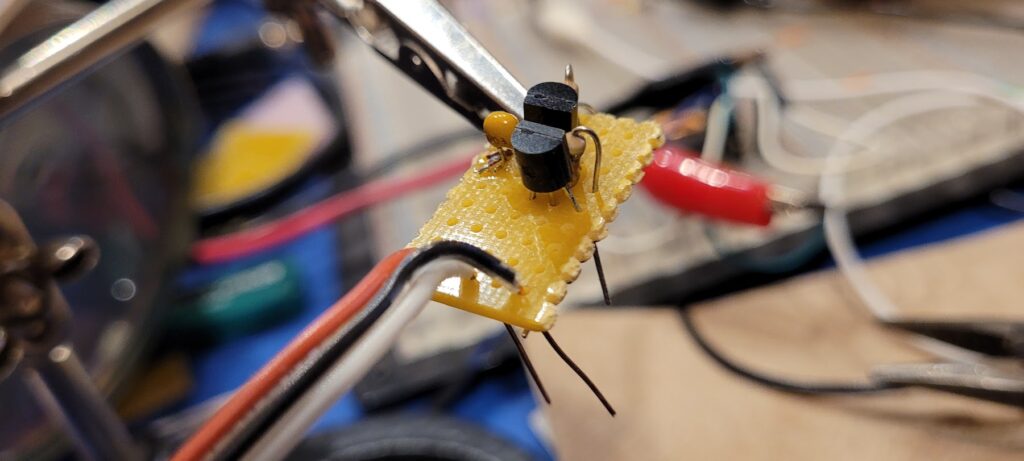
Bend FET leads for ground rail, collector net, and output.
Back on the underside of the board the FET leads can be bent flat against the perf board in parallel with the ground rail, the collector output of the input stage, and along the path of the output lead.
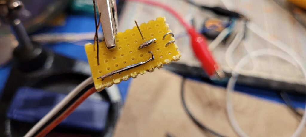
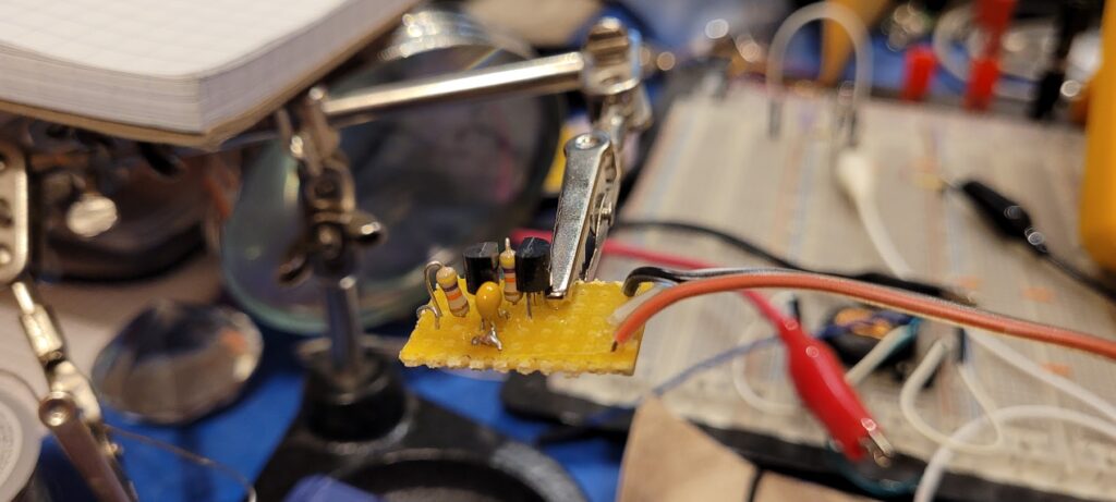
Solder the gate to finish off the collector net; prep ground rail.
At this point all of the parallel leads have been pressed and bent together. Some of them (the ground rail especially, and the output lead) are “a little squirrely” so I save them for the next step where I plan to use some clips as helping hands to get them soldered up cleanly.
Also, in keeping with the input-to-output flow of work, I soldered the gate to the collector net finally completing the input section.
Solder ground rail first pass; prep open drain output.
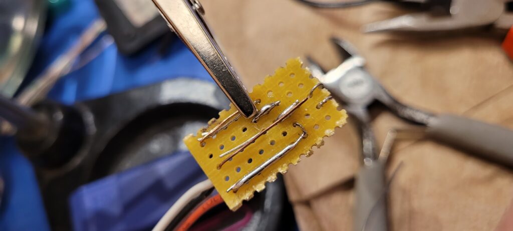
With a bit of patience and a strategic placement of the alligator clip I made a first pass at soldering up the ground rail. That’s enough to hold it in place and keep it tidy while working on the output line.
Open drain output and ground rail done.
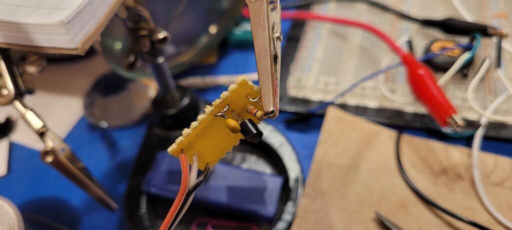
Finally, I soldered and trimmed the output line and reheated the ground rail. That completed all of the nets! Now is a good time to inspect the work and do any final clean up that’s required.
Finished view from the top, ground rail side.
Finished view from top, positive rail side.
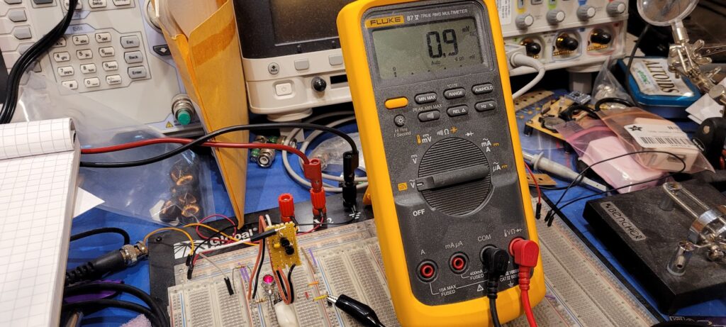
Smoke test; input open.
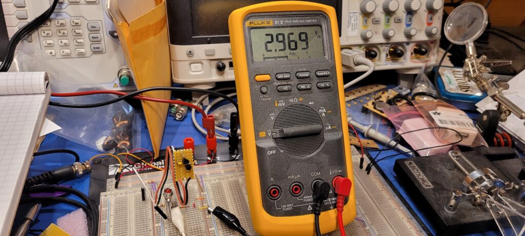
Satisfied that the circuit was correct and anxious to move forward I hooked it up in place of the original prototype on the bread board, turned on the power and the meter, and made a quick test. With the input open the output is also open.
I notice that the numbers are a little different, but not by much, and I expect that having scavenged the parts for this build from those that were used in the breadboard, and that breadboards are notorious for acting differently than soldered circuits, I paid it no mind.
Open for open is GOOD!
No escaping magic smoke!
next test…
Smoke test; input weakly grounded.
Next I put the weak ground lead through the input terminal and I expect the circuit to close.
It works! The circuit closes, the LED comes on, and still no magic smoke!!
…but did you spot the measurement error?
Just now I realize why the numbers are slightly off.
It turns out that in my excitement I put the meter in ACV mode instead of DCV. At first I was very puzzled that I got a stable reading at all… let alone one that was so close to what I expected.
I did some digging. Many (most) meters (this Fluke is one of them) don’t actually block DC when measuring ACV and so will tend to show something close to the DCV measurement when a DC input is present and an AC input is not.
Three takeaways then:
- Hurray! It’s works, and it doesn’t look half bad.
- Be more careful when setting up your measurements. For example, don’t ASSUME that having left your test rig set up it’s all ready to go if you just turn it on; and don’t assume that getting a measurement that’s close to what you expect is a sure sign everything is correct!
- A DVM on ACV will probably (almost) measure a DCV that’s close to what you expect. Who knew?!