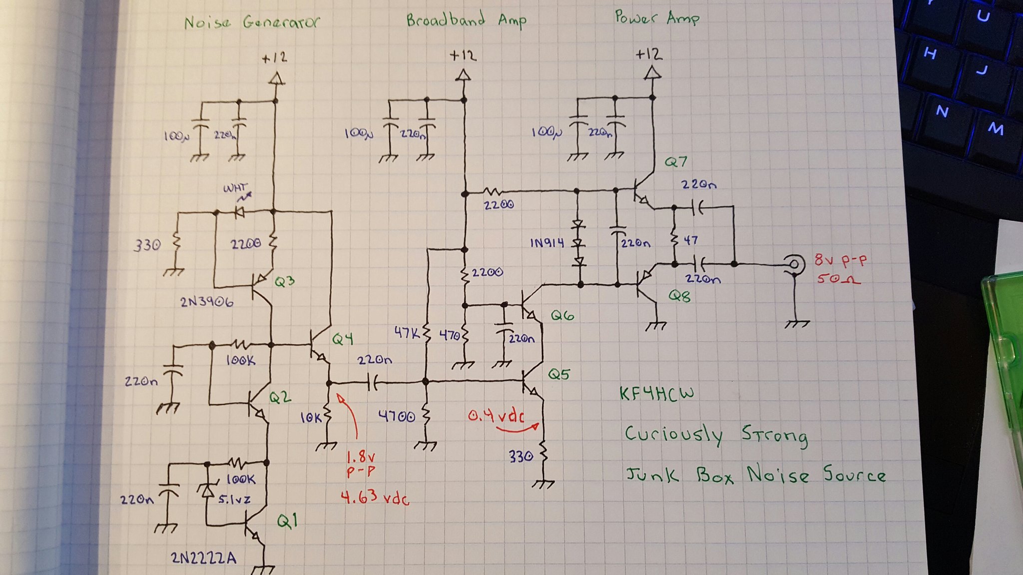
Curiously Strong Junk Box Noise Source in an Altoids Tin
Why build a noise source?
A good noise source is handy around the lab. It’s useful for testing radio gear, characterising filters and amplifiers, and the list goes on…
There are many schematics out there for noise sources, you can buy kits for them, or you can spend a lot of money and buy a calibrated noise source ready-made. Most of the circuits I found use MMICs to boost a weak noise signal up to a usable amplitude. I have some of those MMICs around (typically $8 parts) for special projects but I wanted to play around with some ideas I had for various circuits and I thought it might be fun to see how far I could push junk box parts that anybody might have laying around their lab.
Since I enjoy working in HF and below I thought a noise source that produces a reasonably flat 1/f output up to about 50MHz would work great. So that’s what I set out to build.

Theory of operation…
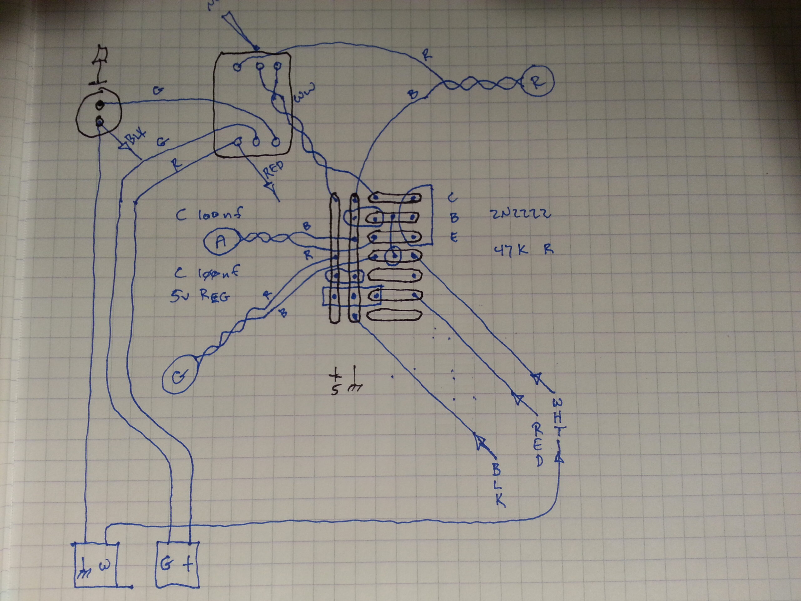
Like most noise sources this one starts off with a reverse biased diode — in this case a 5.1 volt zener — and then greatly amplifies the noise it generates in a broad band amplifier. This sounds easy enough, but I tried to take it to the next level using several circuit tricks that are more commonly found in high performance receiver, instrumentation, and test equipment designs.
There are three basic sections. The first is a noise generator which captures the weak noise of a zener diode and amplifies it to a useable level. The second section is a broadband amplifier which isolates the noise generator and boosts the signal a bit more. The final section is a power amplifier that converts the moderately high impedance output of the second stage to a low impedance output capable of driving 50 ohm loads.
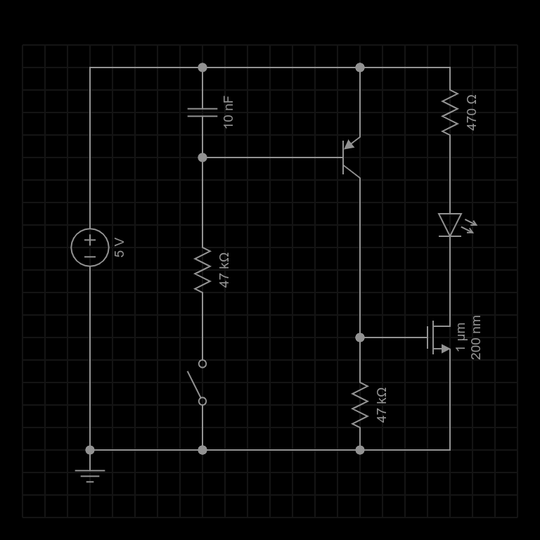
Q1 – Noise Generator
A 5.1 volt zener diode is just barely brought to breakdown by a 100K resistor in a self-biased common emitter amplifier. The noise from the zener is fed into the base of Q1 and coupled to the emitter by bypassing the high side of the zener to ground through a 220nf cap.
Q2 – Cascode Noise Stage
The goal is to provide as much gain as possible because the noise voltage coming from the zener diode is extremely weak. High gain common emitter circuits tend to suffer from the Miller effect which essentially magnifies the apparent size of the parasitic capacitor between the base and collector causing higher frequencies to be attenuated.
In order to preserve as much bandwidth as possible we use a cascode stage. This is essentially a common base amplifier coupled directly to the collector side of the common emitter amplifier. It effectively “hides” the inverted output signal from collector of Q1 so that it can’t get coupled through that parasitic b-c capacitor to the base of Q1 and reduce the gain at higher frequencies.
The interesting thing about this cascode stage is that it is also self biased. This is unusual, but it works in this case because the load for the noise amplifier is a constant current source. At DC, the constant current source essentially forces both Q1 and Q2 into conduction by driving their collector voltages toward the positive rail until the current flowing through them reaches the set point. Q1 and Q2 both have a 100K resistor between their collector and base and they are of the same type so they have a tendency to reach equilibrium.
This technique eliminates the need for the separate bias network that is typically found in cascode amplifiers. One of the reasons we can get away with this is that the signal being amplified is so small that it never pushes the transistors very far from their DC operating point. Removing these extra components helps to eliminate any of the “colors” those components might add — by which I mean that any additional components in this stage might boost or attenuate certain frequencies and this is something we want to avoid.
Q3 – Constant Current Source as a High Impedance Load
The gain of a common emitter amplifier is determined by the difference between the emitter impedance and the collector impedance. The cascode stage (Q2) is effectively invisible in this respect. The emitter of Q1 is connected directly to ground so it’s impedance is already about as low as we can make it. In order to get a high gain we want to make the collector impedance as high as possible.
In this design I’ve used a constant current source as the load. This trickery is very interesting because from a DC perspective the constant current source might as well be an ordinary resistor, but from an AC perspective it looks (almost) like an open circuit. One way to think of it is like a huge, nearly perfect inductor. An inductor resists any change in current flow and so it presents a high impedance to AC signals. A constant current source looks to the AC signals like it is an infinitely large inductor that just “wont budge” when the voltage changes.
Unlike an impossibly large inductor that would have problems with self resonance and self resistance, the constant current source appears by comparison to be almost perfect.
The combination of a direct connection to ground at the emitter of Q1, and a connection to an extremely high AC impedance at the collector of Q2 results in a very high gain. In a perfect world the gain would be infinite — but nothing is perfect, so in the real world we get instead a useful but extremely high gain.
To set up the constant current source we need a stable voltage. In this case we use a white LED which doubles as an “ON” indicator and develops about 3.4 volts. Most of the LED current sinks through a 330 ohm resistor to ground. The LED voltage appears at the base of Q3 developing a stable voltage across Q3’s 220 ohm emitter resistor. Q3 is forced to conduct just enough to keep this voltage stable and thereby establishes a “fixed” current proportional to the LED voltage (minus the b-e drop) and emitter resistor.
Q4 – Buffer Amp
The high gain noise amplifier does a fantastic job typically resulting in a noise voltage well in excess of 350 millivolts peak-to-peak but there is a problem. The impedance at the collectors of Q2 and Q3 is extremely high and the gain depends on that high impedance. So, we need a buffer to bring this impedance down to a more practical level.
The noise signal is direct coupled to the base of Q4 which is an emitter follower with a 10K emitter resistor. This establishes a reasonable DC bias point for Q4. The actual impedance at the output is dominated more by the bias network of Q5 and is still reasonably high (about 4500) to preserve as much gain as possible in the noise generator stages.
Note also that the relatively high impedance at the output of Q4 and input to Q5 helps to swamp out any unwanted frequency shaping effects of the 220nf coupling capacitor between those transistors. I had experimented with using a Vbe multiplier and some other options to preserve a direct coupling at this stage but ultimately found that a conventional approach was sufficient. I may still revisit this in future versions.
Q5 – Common Emitter Voltage Amp
The signal at the output of Q4 is nominally 350mv p-p though it is possible to observe spikes to 1.8v or so. The goal is to get the noise signal as close to “rail-to-rail” as is possible so some additional voltage gain is required. This presents some challenges.
This being a noise generator I was tempted to ignore the fidelity of the output stages — after all, is it even possible to measure THD% on a pure noise signal?? Along the way I discovered that linearity actually matters quite a bit if you care about the shape of your noise signal (more on this later) and this imposed some hard limits on just how much and what kind of amplification can be used.
A perfect linear amplifier would preserve every spike in a 1.8v p-p input signal and would translate it to a corresponding 12v p-p output at 50 ohms. That would require a gain of about 6.67.
Of course, it’s not really possible to build one of these perfect amplifiers. For one thing, we’re going to use a cascode stage here to preserve bandwidth and that will take out a few tenths of a volt. For another there’s the 0.7v b-e drop to consider — so we’ve lost about a volt already (0.2 v-sat of Q6 + 0.7 Vbe of Q5). Then there are similar issues with the final output stage and so forth.
After much experimentation the best overall result was achieved by biasing Q5 on the low side of class A with a gain of about 6.7. This means that most of the noise signal is amplified linearly but on some of it’s excursions the amplifier is forced into cut-off or saturation momentarily.
The DC bias for Q5 is set up by a 47K and 4700 ohm resistor divider at it’s base. The 330 ohm emitter resistor sets the bias current at about 1 ma which works well with the 2200 ohm load to set the gain.
Note that there is no bypass cap on Q5’s emitter resistor. This keeps this stage nice and stable by bucking any errant oscillation attempts and establishes the gain very deterministically. However, at some point in the future I may rethink this design and explore the use of a small bypass capacitor (50-100pf) to boost the gain at higher frequencies. This will change the 1/f slope of the circuit but if a good response can be achieved at a lower slope that might be desirable.
Q6 – Cascode Voltage Amp / Driver
The bias point for this cascode stage is established with a 2200 and 470 ohm resistor. AC at the base is bypassed to ground with a 220nf cap. This is a more conventional treatment for a cascode stage. Note that the bias network for this stage has a much lower impedance than the bias network for Q5 intentionally. At Q5 it is important to preserve a relatively high input impedance, but since Q6 is essentially acting as a common base amplifier we want a low impedance in the bias network. I could have chosen smaller resistors here but I didn’t want to burn “stupid amounts of power” biasing this transistor and the 2200/470 resistors were handy and seemed in line with the rest of the circuit.
The bias point is just high enough to minimize distortion while being as low as possible to preserve a sizeable voltage swing at the output. I established this experimentally at one point using potentiometers to play with the bias points of both Q5 and Q6 to see just how much voltage swing I could squeeze out of the amp while balancing off all of the other factors. In the end it turned out that pushing the limits would result in potential instability and so I reverted to the math and picked handy values that “worked” well enough.
Q7, Q8 – Power Amp
The output impedance of the voltage amp (Q5 & Q6) is much higher than the desired 50 ohm output, so we use a complimentary symmetry pair to drive low impedance loads. This amounts to a pair of emitter followers working opposite sides of the power rails with their outputs connected together. The power amplifier is direct coupled to the preceding voltage amplifier and actually forms part of the load of Q6.
Three 1N914 switching diodes develop a differential bias at the bases of Q7 and Q8. This is stabilized by a 220nf capacitor. The cap isn’t strictly necessary, but it seemed like a good idea to keep Q7 and Q8 locked together on both their inputs and their outputs.
The voltage developed across the diode network is essentially 3 “diode drops” which is always slightly more than the 2 “diode drops” represented by the b-e junctions of Q7 and Q8. The extra “diode drop” appears across the 47 ohm output resistor between the two emitters effectively pushing their voltages apart to establish a low but stable DC current. This keeps Q7 and Q8 in a fairly linear region of operation without burning too much power and also serves to eliminate any thermal run-away since additional current through the 47 ohm resistor would increase the voltage between the emitters and begin to shut off the current flow.
The AC signal at the output of Q7 and Q8 is coupled through a pair of 220nf capacitors to the output. The difference between the emitter voltages at Q7 and Q8 are also stabilized by the network (although at a lower capacitance of about 110nf) so that if one or the other is driven into saturation or cutoff they will none-the-less follow each other through the clipping event.
The ability to drive the output from both rails ensures that the output signal is as symmetrical as possible even if the load itself is not.
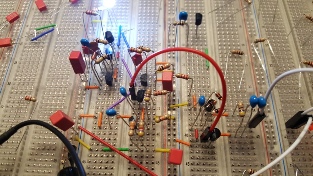
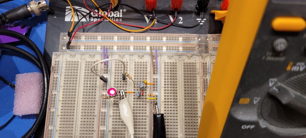
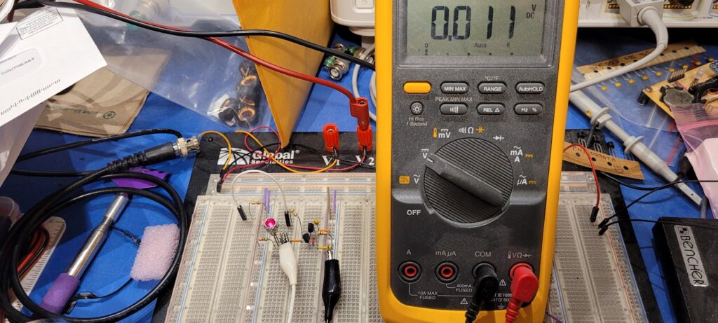
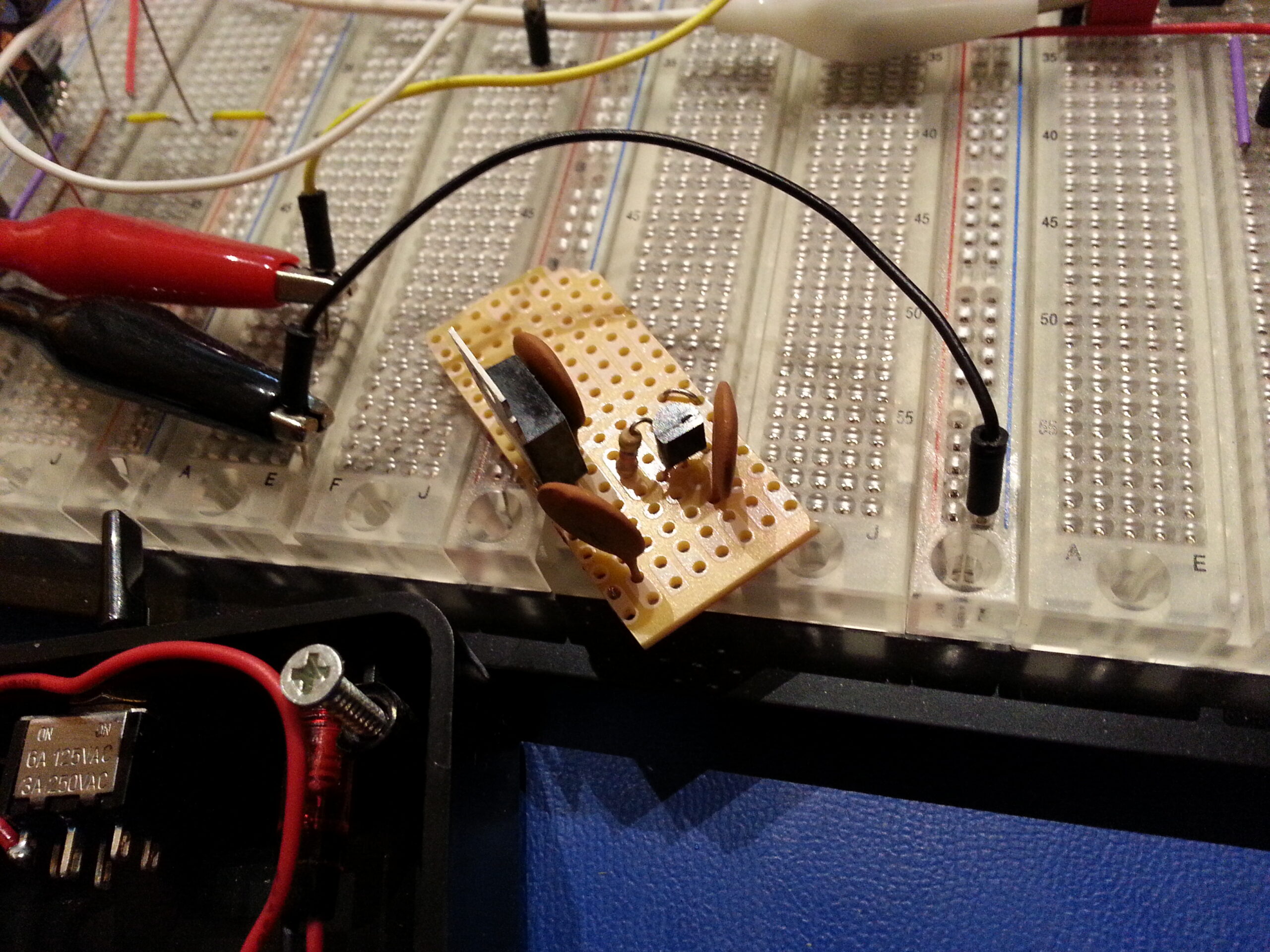
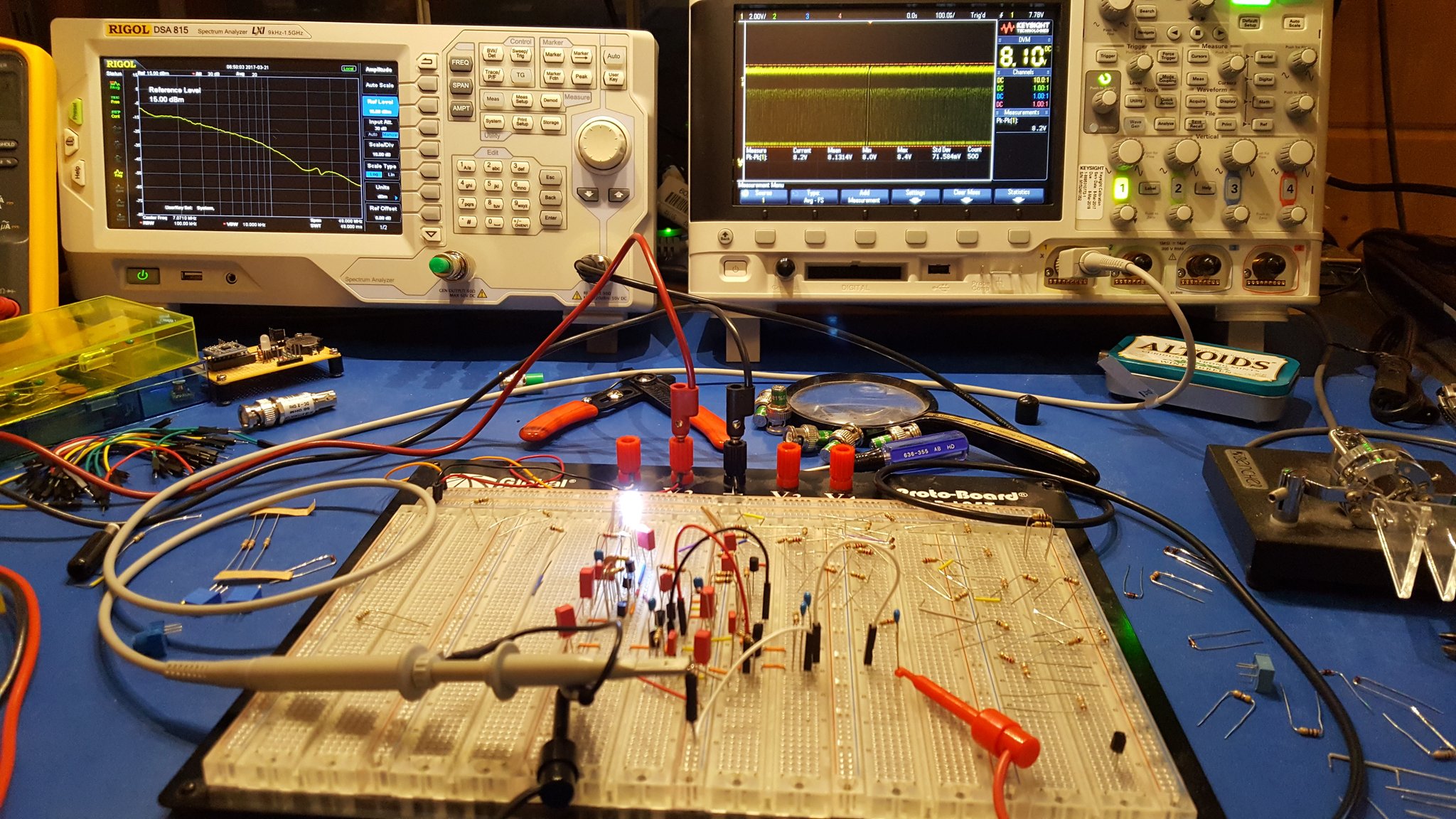
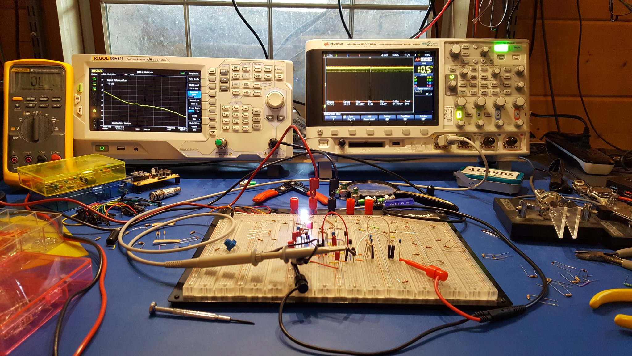
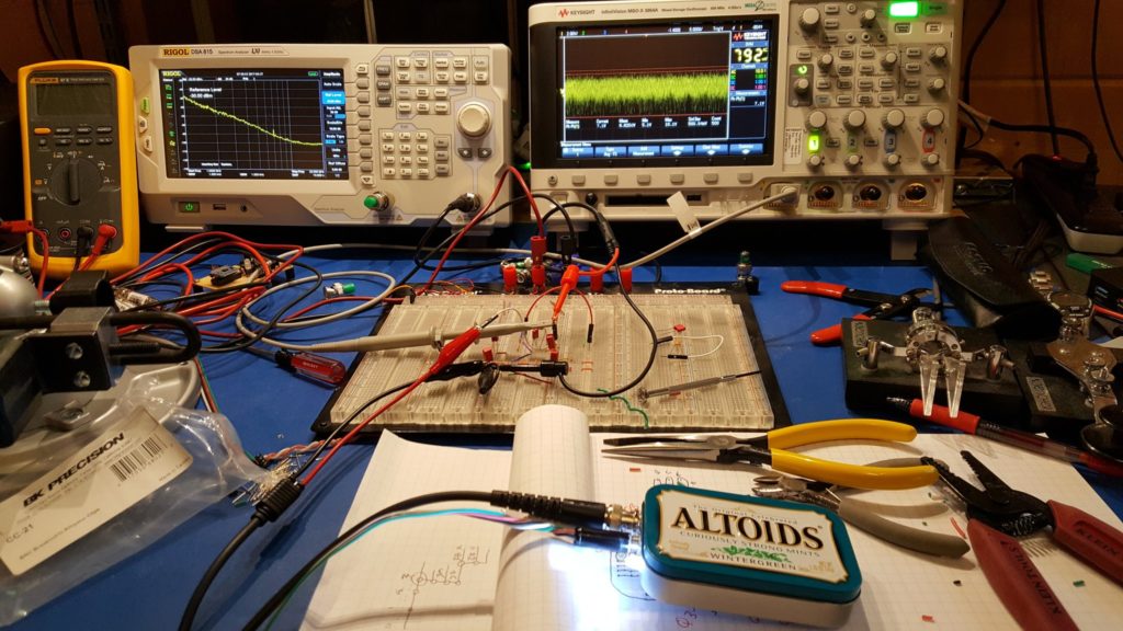
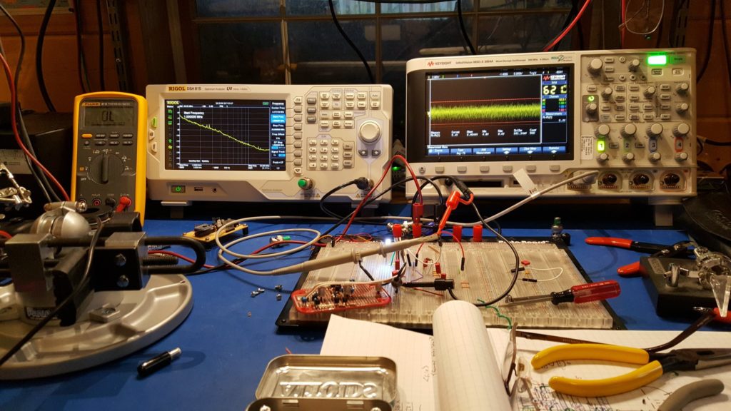
There is no substitute for playing with circuitry on a breadboard.
Curious Lessons Learned…
It turns out that reinventing the wheel teaches you a lot about wheels. Conventional wisdom aside, I highly recommend reinventing wheels wherever possible — there just aren’t enough people in the world who really understand wheels, and that number grows smaller every day.
I learned a few interesting things on this particular wheel.
For example, linearity matters even when you’re only amplifying noise! The goal of a noise source is to have a predictable (if not uniform) frequency mixture that is as close to “flat” as possible. This is important because it allows you to throw your noise source at the input of a device and compare that “known quantity” with the output of that device. If the input (your noise source) is wild and unruly then it’s nearly impossible to know what part of the output is “weird” because of your noise source, and what part of it is “weird” because of the device.
One of the first versions of this circuit used a constant current source to boost the gain of the second amplifier stage with the intent of driving the output to saturation at random intervals instead of simply amplifying the already random but somewhat more linear noise from the zener diode. The logic was that this arrangement would allow the output to swing essentially from rail-to-rail providing a high intensity broadband noise into virtually any load.
It turns out that sort-of works…

When you amplify a uniform noise signal non-linearly you create unwanted artifacts in the frequency domain.
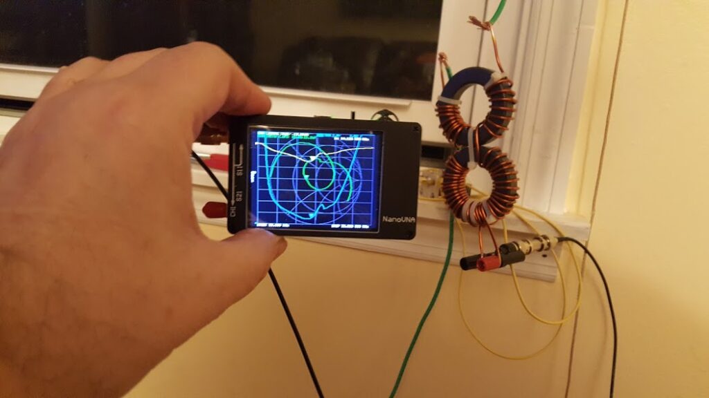
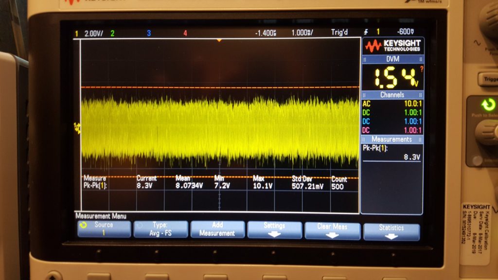
If you look carefully (zoom in) at the trace on the spectrum analyzer you will see that there are some definite curves to the spectrum of the noise output. Some of the bumps and valleys are subtle — maybe even subtle enough to ignore — but some of them are fairly aggressive. What we want to see here is essentially a straight line sloping down from the left to the right. Clearly, that’s not what we have here.
What’s worse is that this arrangement is unstable. If you take a look at the waveform on the oscilloscope you’ll see that it spends a lot of it’s time at the top rail, and that there is a bit of randomness in the middle, and that the bottom rail is populated less aggressively. What you’re seeing is almost, but not quite, what was intended. In a perfect world this design would have had the top and bottom rail equally populated and there would be an evenly distributed ridge of randomness between them where some of the random transitions of the waveform would happen in between the rails. The waveform would spend random amounts of time at the top rail, equal but random amounts of time at the bottom rail, and in between would “change it’s mind” almost as often as it swings back and forth.
It turns out that it is very hard to get the system biased correctly to achieve that result. Indeed if you do manage to get that result the system will tend to drift off of it within a few minutes and almost certainly will be “unbalanced” if you turn it off and on again.
Actually, that presented me with an interesting challenge and for a while I almost set about fixing it — I thought it would be fun to figure out how to make the circuit self stabilizing so that I could achieve precisely this kind of randomness… but I realized after a while that it wasn’t going to give me what I wanted even if I did manage to stabilize it.
Along the way to that point I did discover an alternative that was almost good enough and even provided more energy in the higher frequencies…

A possible solution was to produce very short high amplitude spikes at random.
One possible solution to the instability actually produced a pretty good spectrum. It had more energy in the higher frequencies and an attractive “flat spot” in the mid spectra. In this case, still using a constant current source in the amplifier stage, I allowed the system to settle on the top rail and then randomly pull the signal down to ground for very short duration spikes at random intervals.
This turns out to work pretty well because any short duration spike must contain energy at a very large number of frequencies. So, generating a lot of short, high amplitude spikes at random intervals is potentially a good way to create broadband noise. Not only that, but this circuit is a lot easier to stabilize because it’s essentially biased to sit on one rail and “bounce” off of it violently and at random. If you use the average output voltage to “tune” your bias then the random noise coming from your zener diode can be made to cross a threshold at some reasonably uniform rate with each crossing producing a spike.
However, there is a problem with this. Although the spectra looks nice it is definitely not uniform in the way we expect or hope. Not only that, but if you think about applying this to the input of some device with a moderate frequency response it makes you wonder whether the results will tell you anything useful. What if the device simply refuses to respond to the spikes in the noise signal at all? What if that causes the output to be much lower than you would expect?
I think this is a reminder that there are many ways to create a particular spectra and they are not all equal. The spectrum analyzer in this case is showing a curve that looks promising with energy apparent at all of the desired frequencies and in something close to the desired amounts… but the character of the signal being described is hidden by the effects of averaging and windowing. The actual energy spectra is more “bursty” than we actually want. Instead we want something that is smooth – containing a good mix of energy at all frequencies all of the time, or at least as close to that as is possible.
Still, this was interesting and there may be some good applications for it.
Who knew that there would be so many “kinds” of noise with nearly indistinguishable spectra and that each would potentially have it’s own applications.
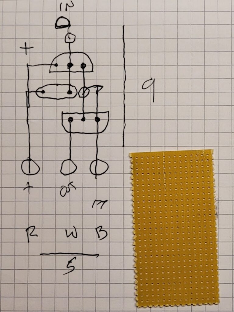
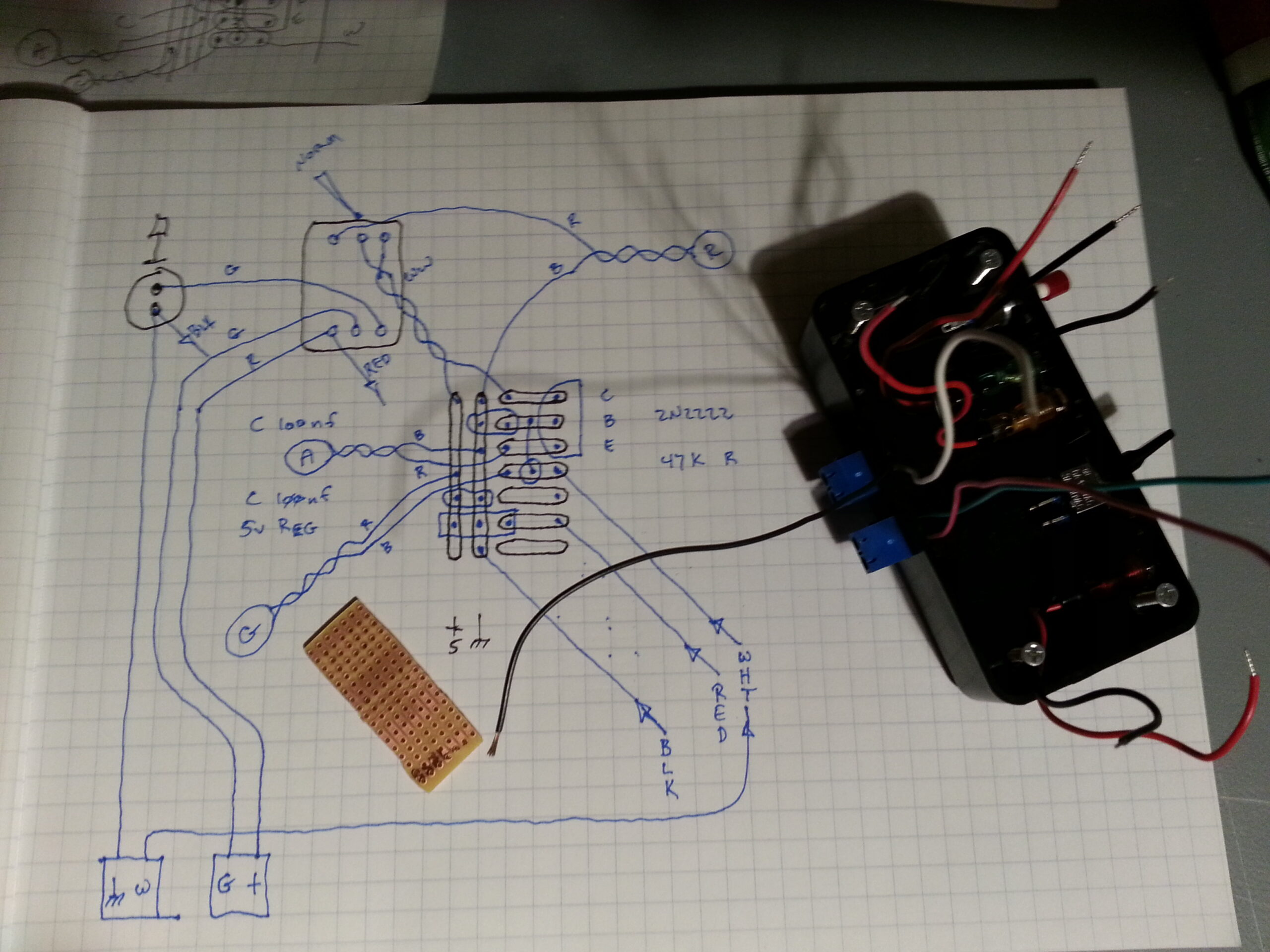
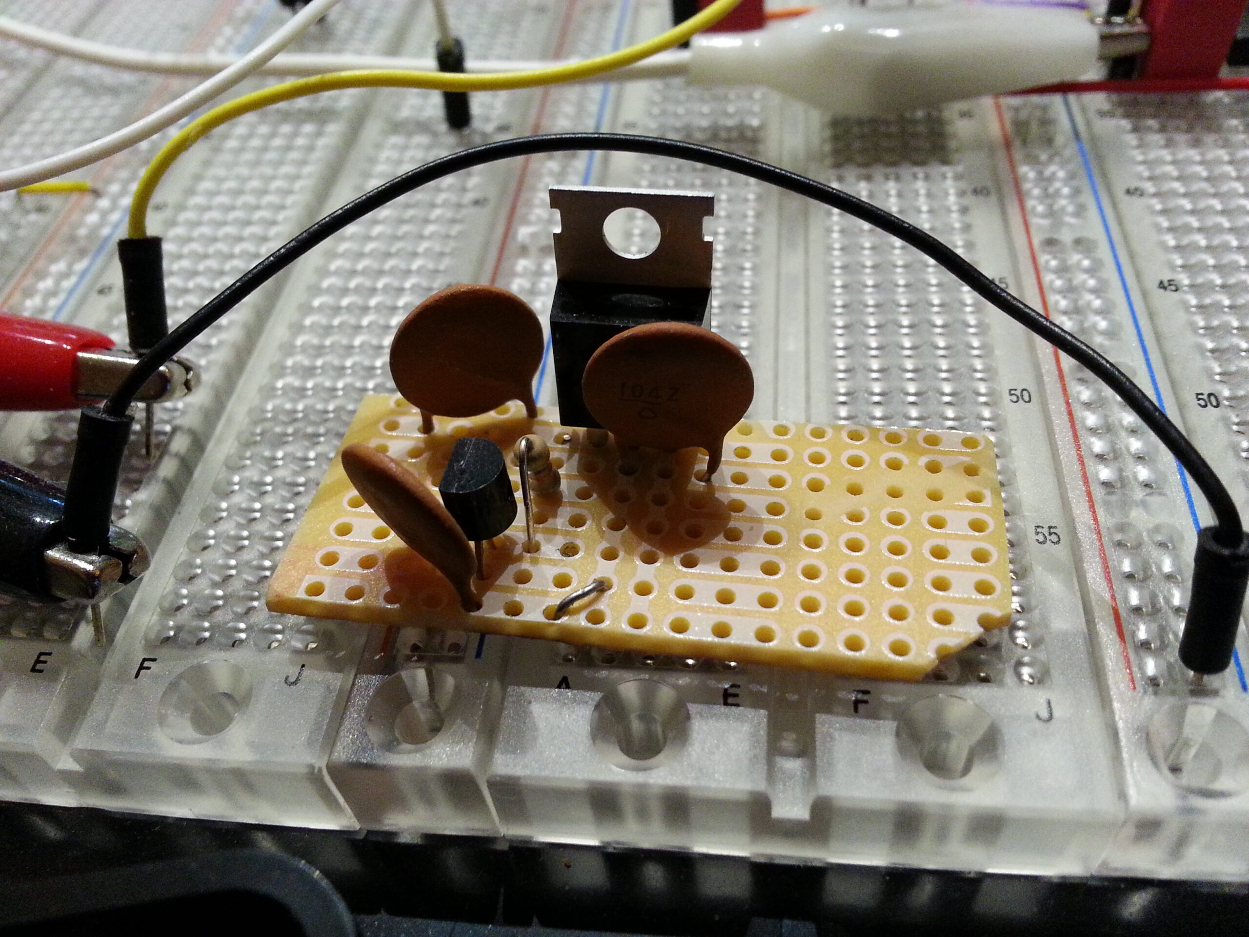
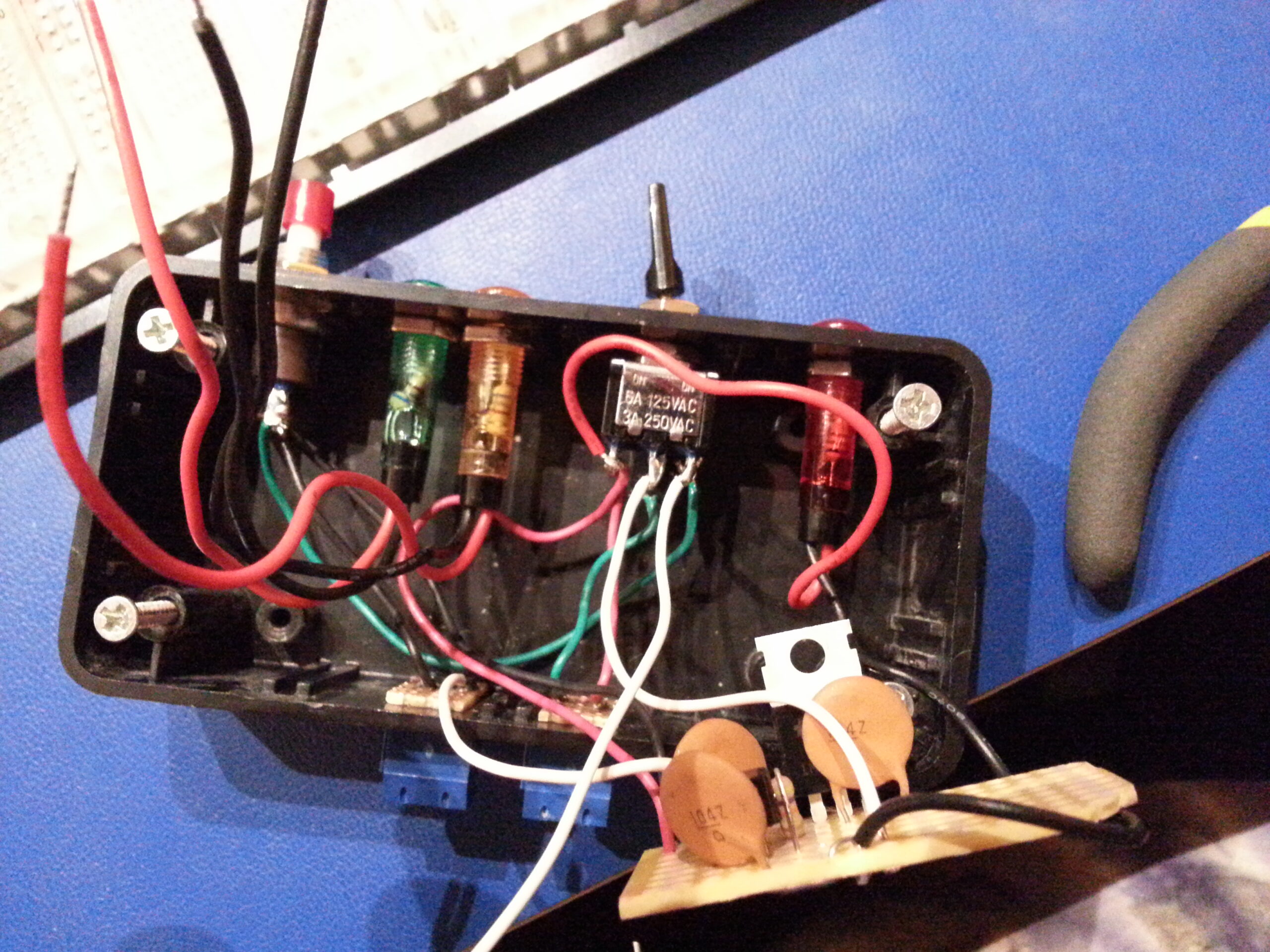
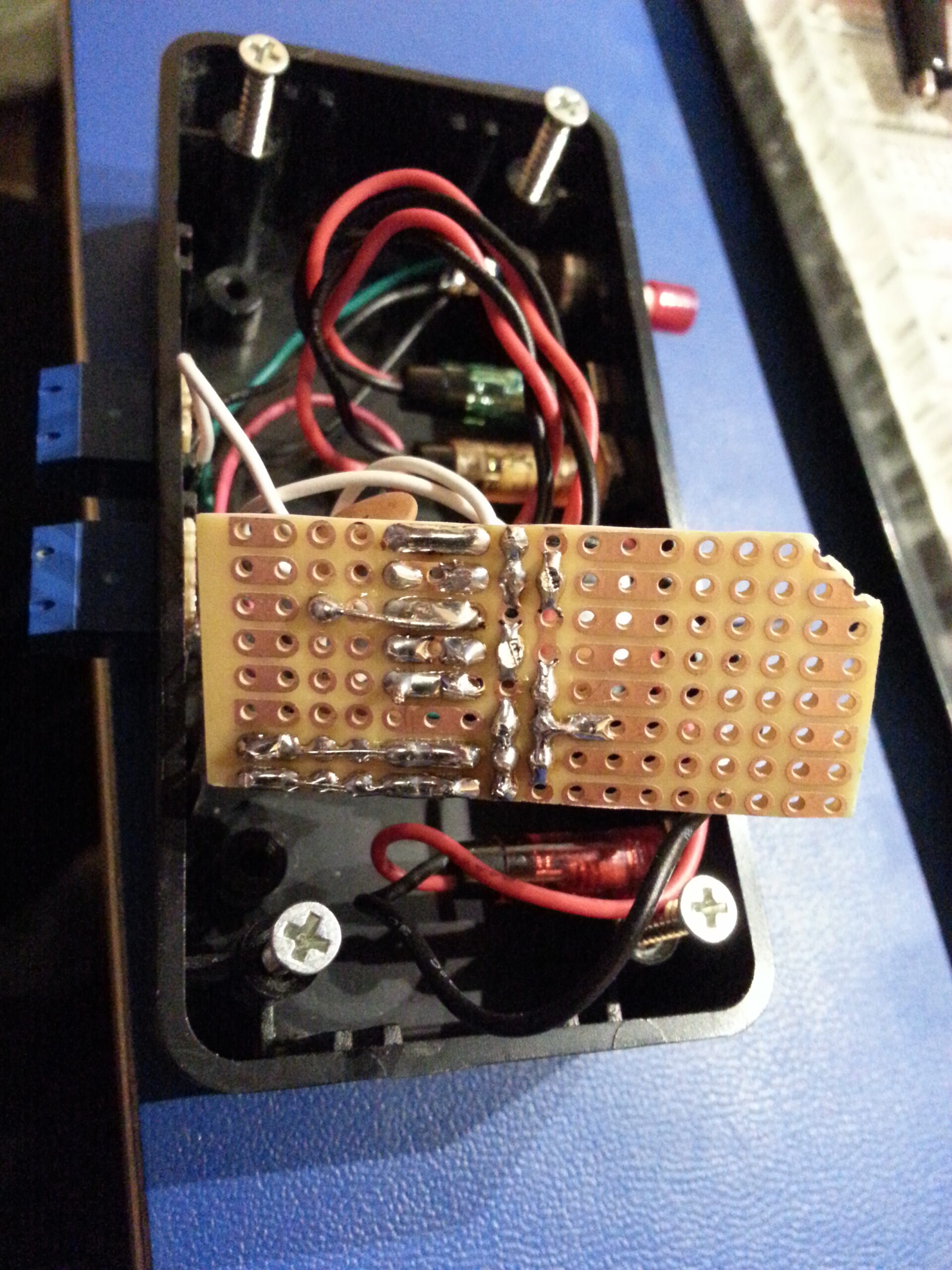
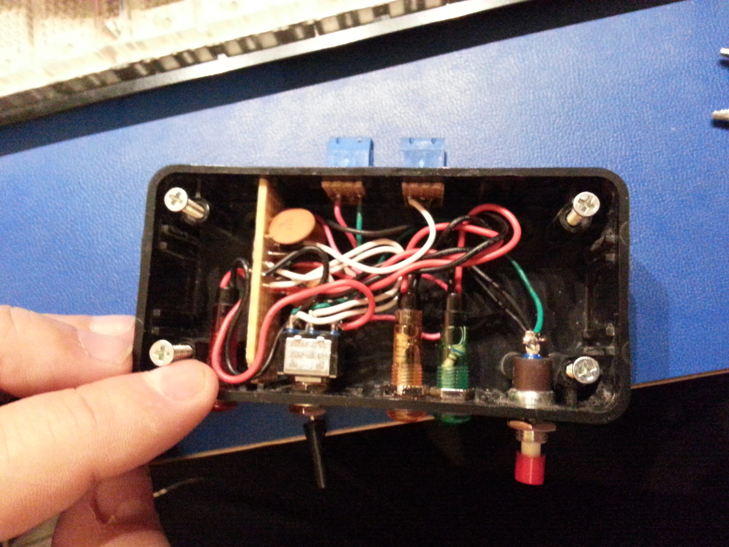
Construction
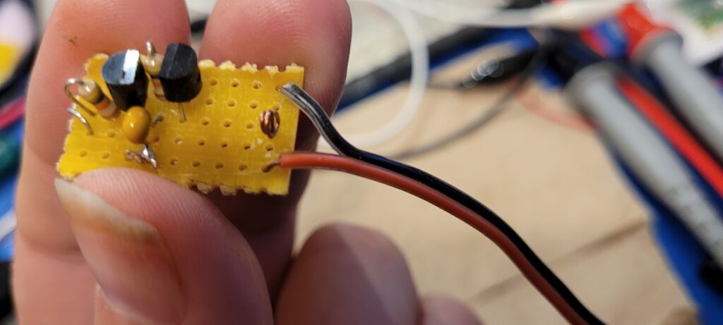
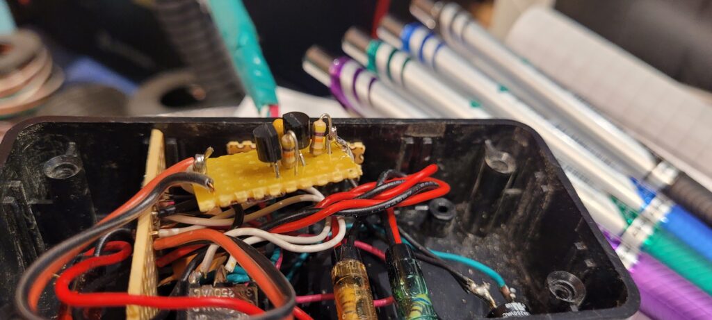
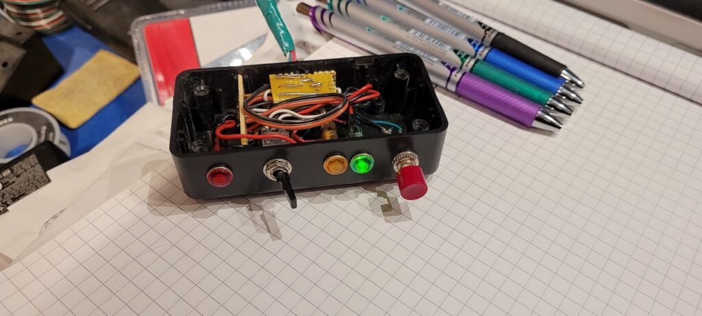
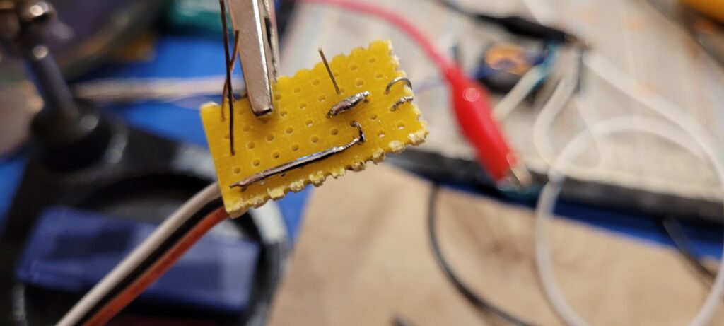
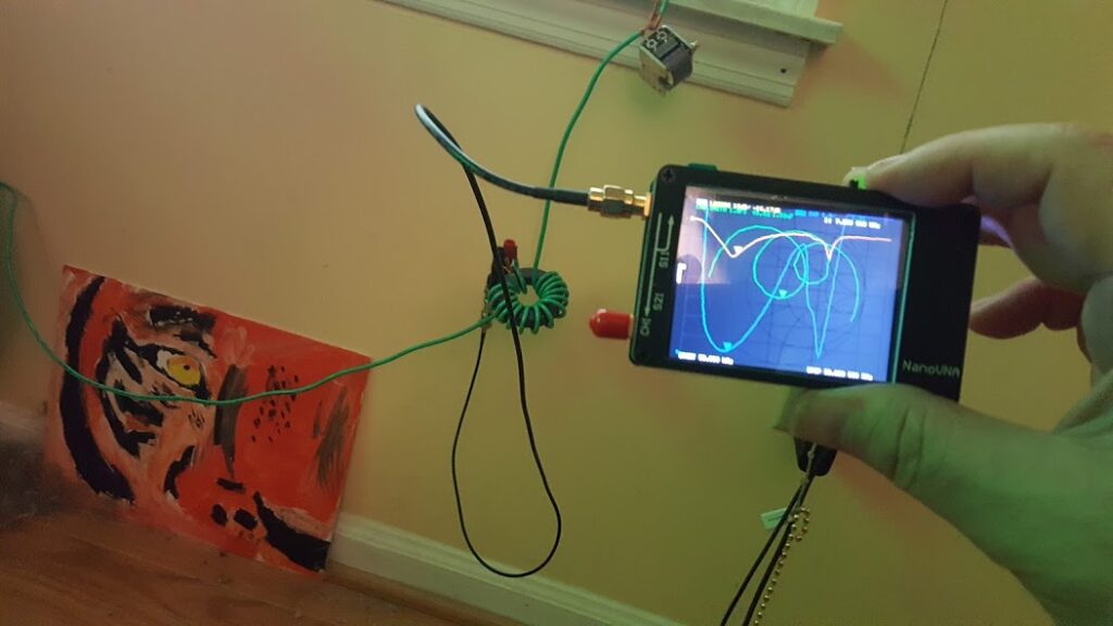
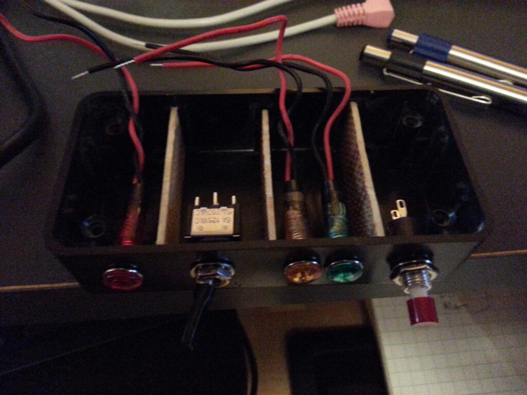
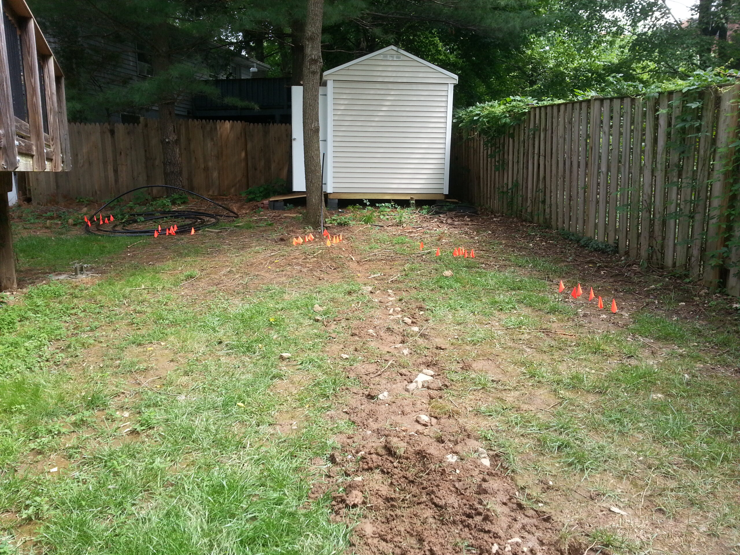
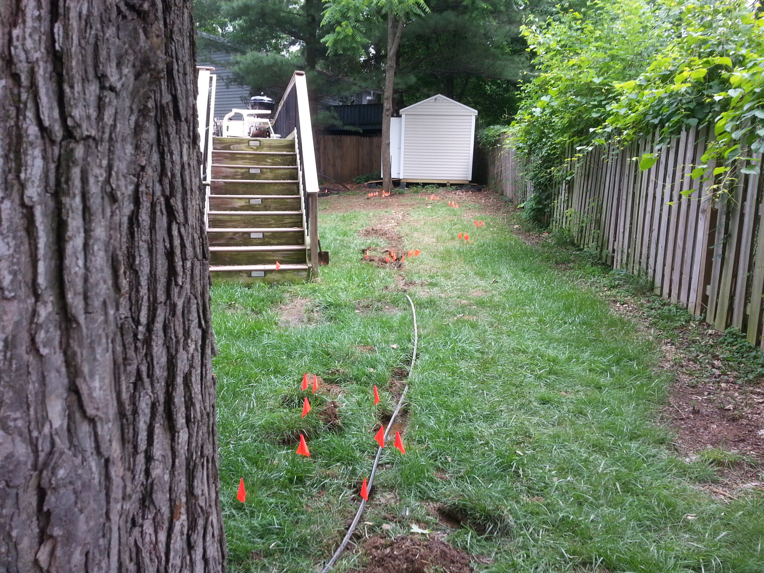
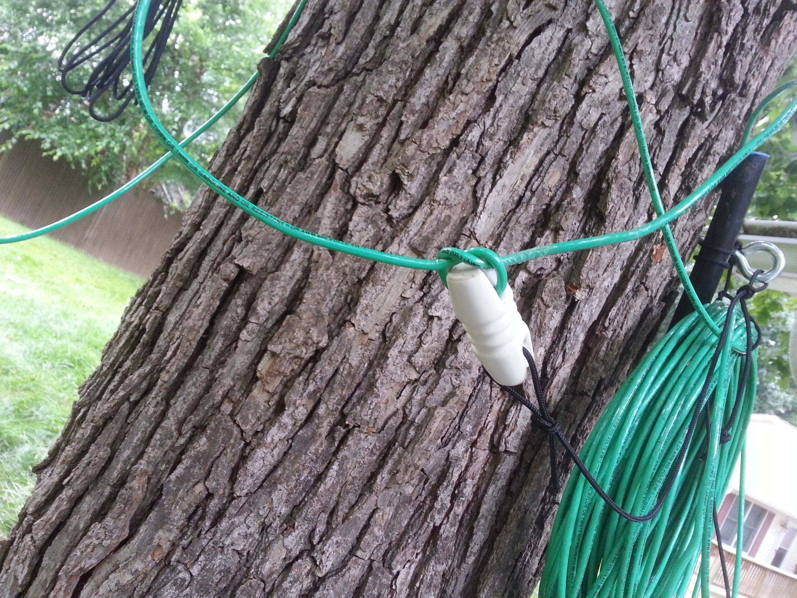
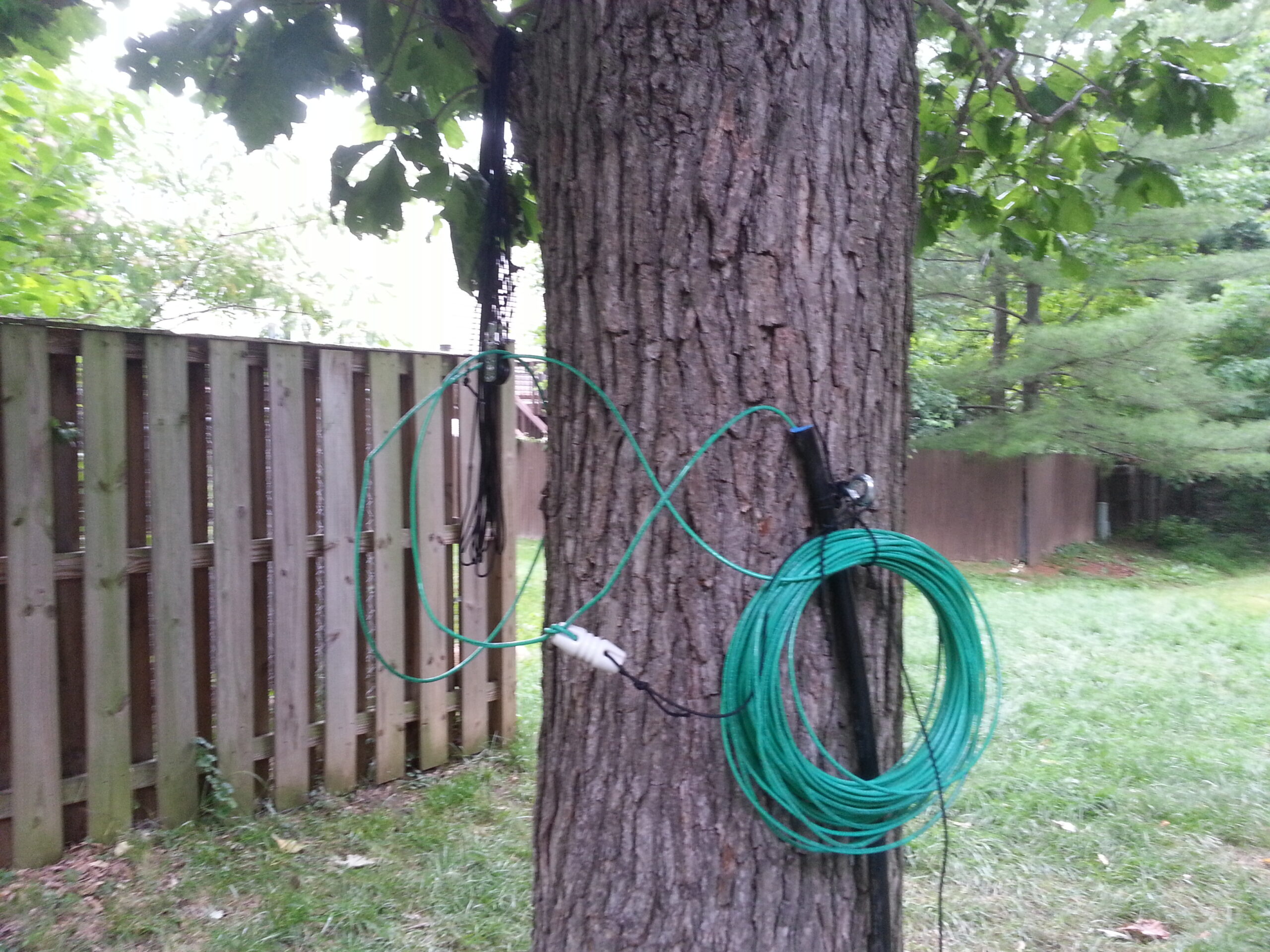
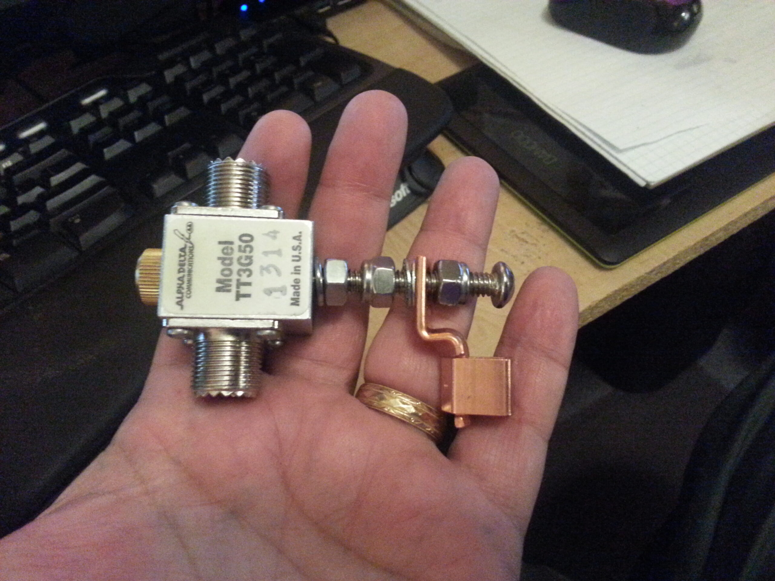
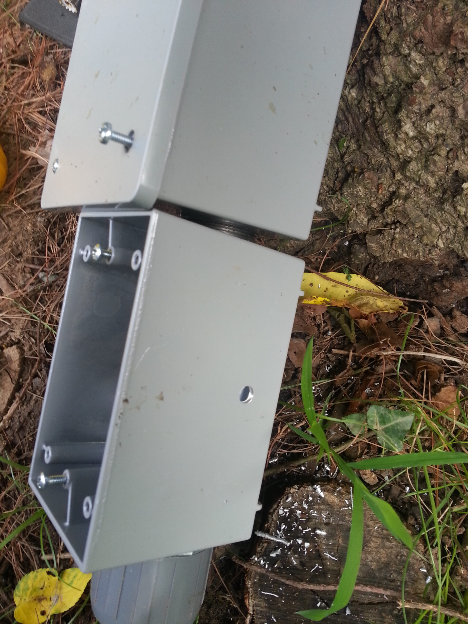
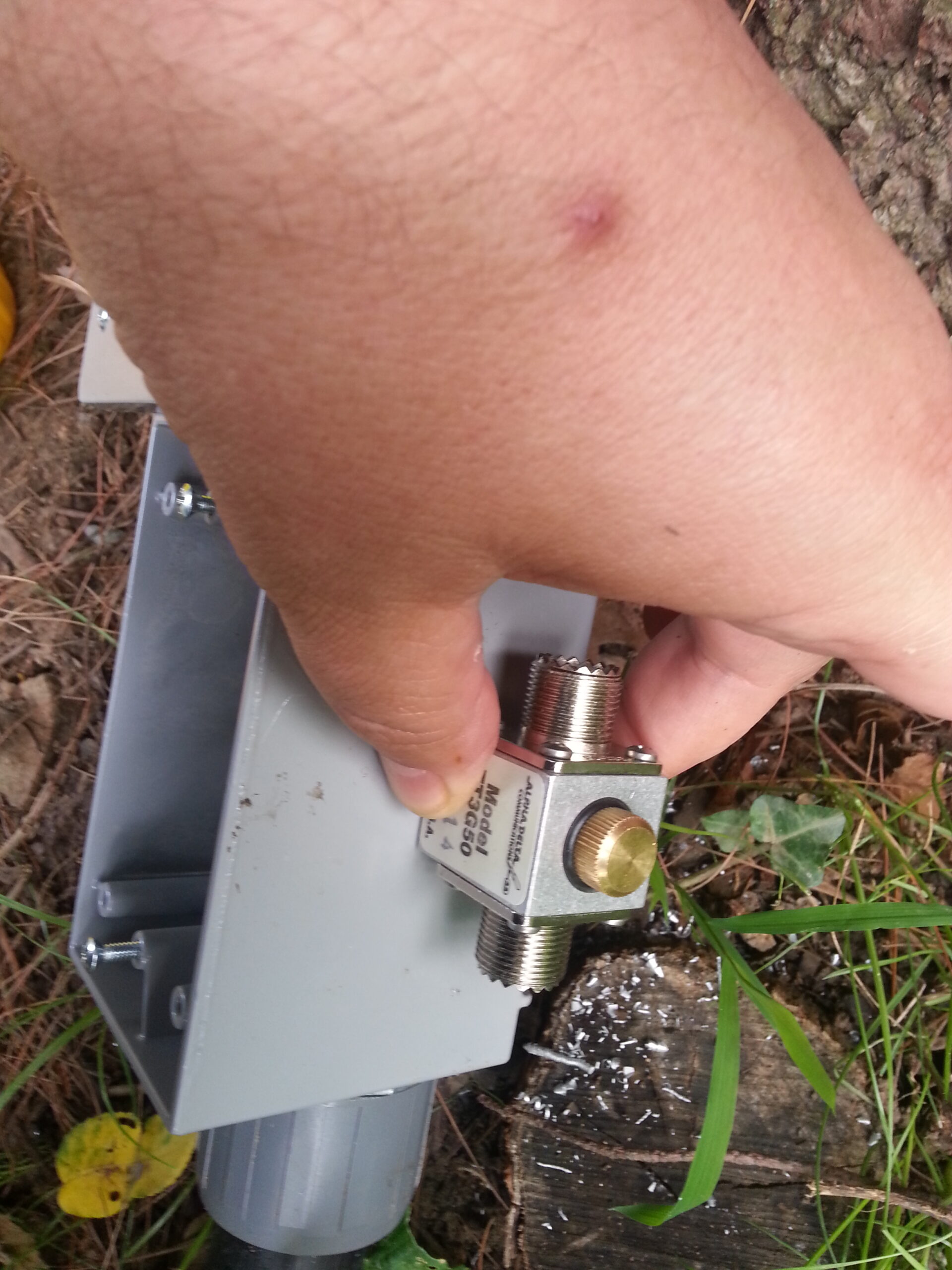
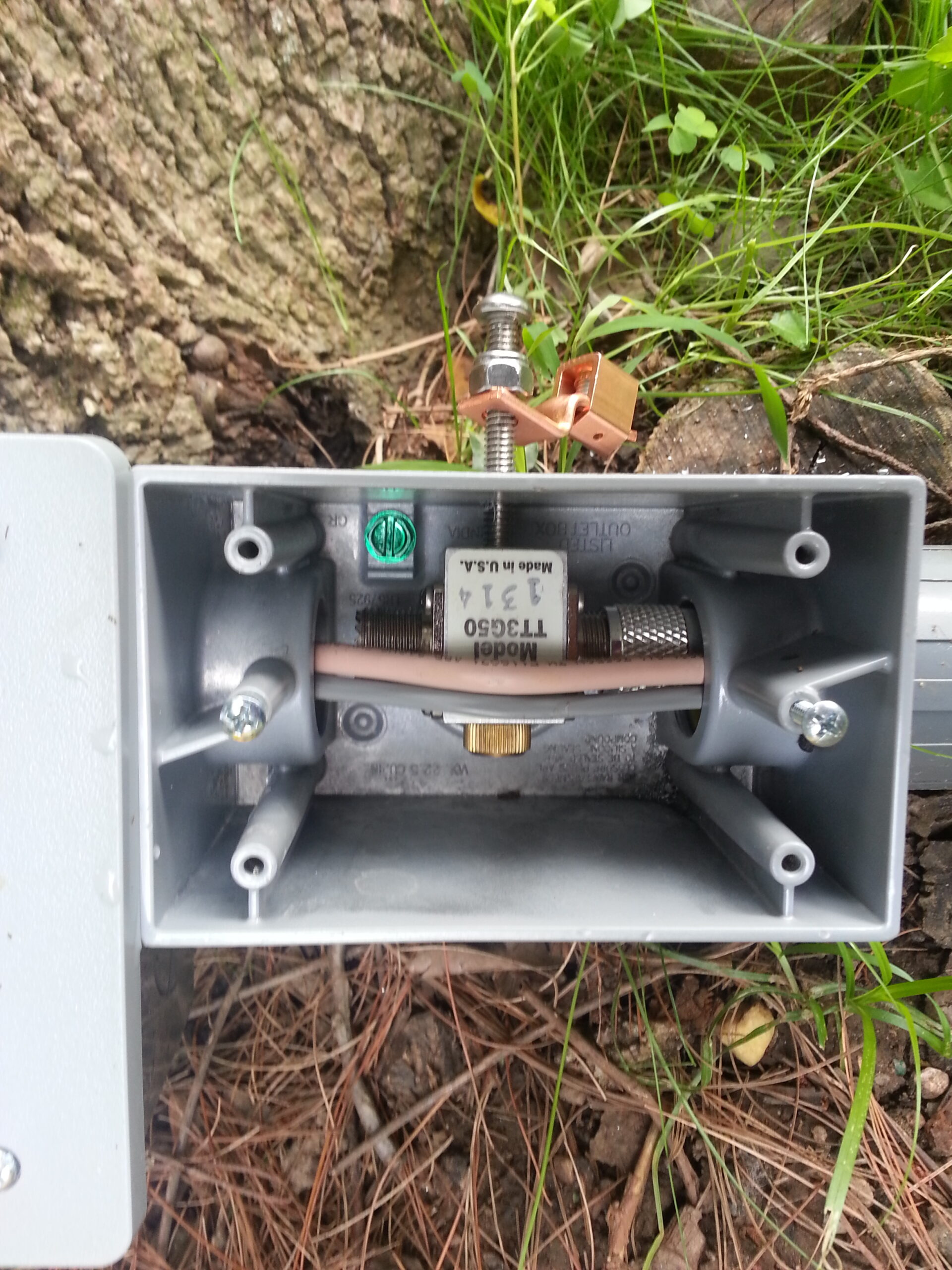
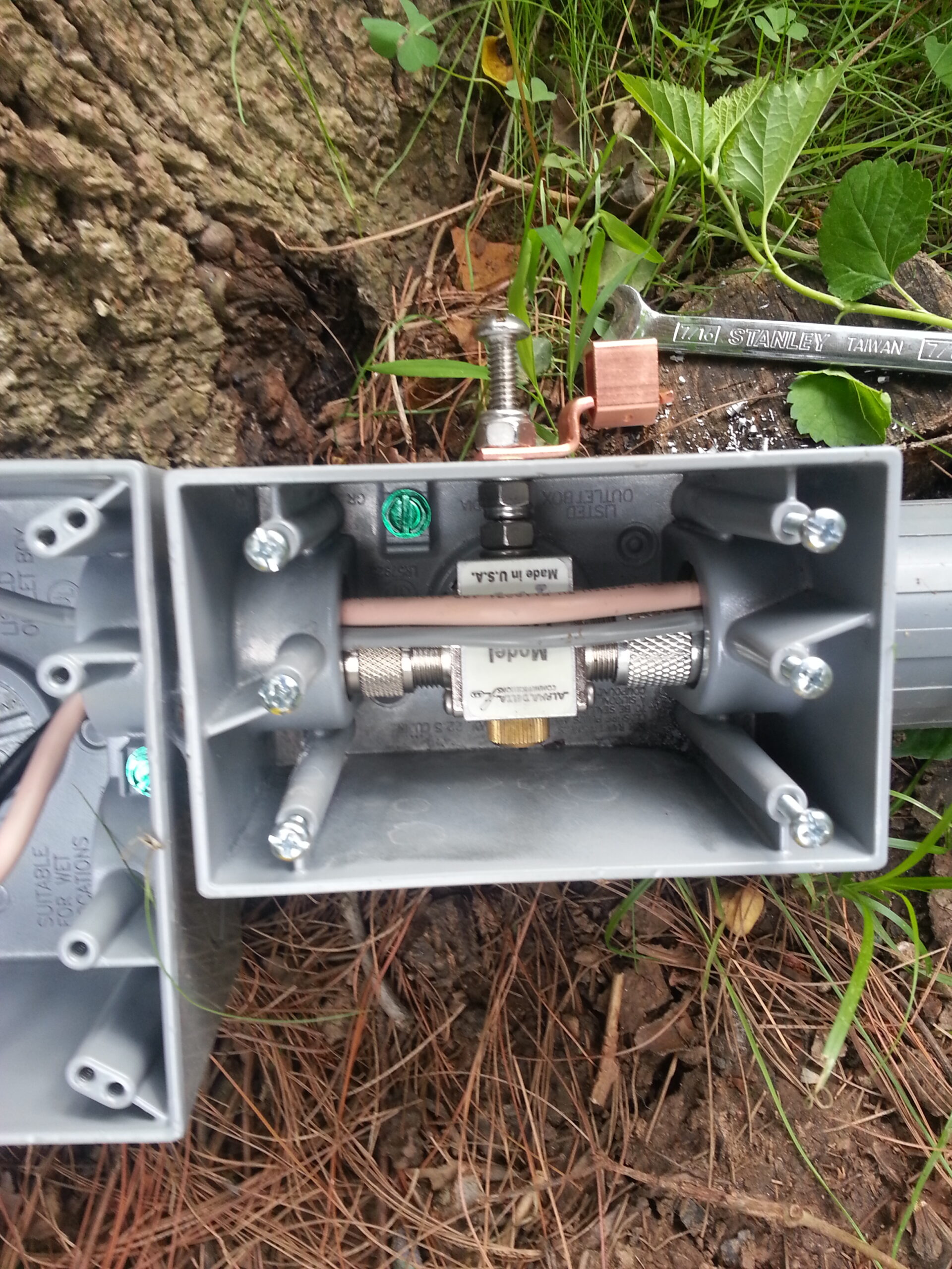
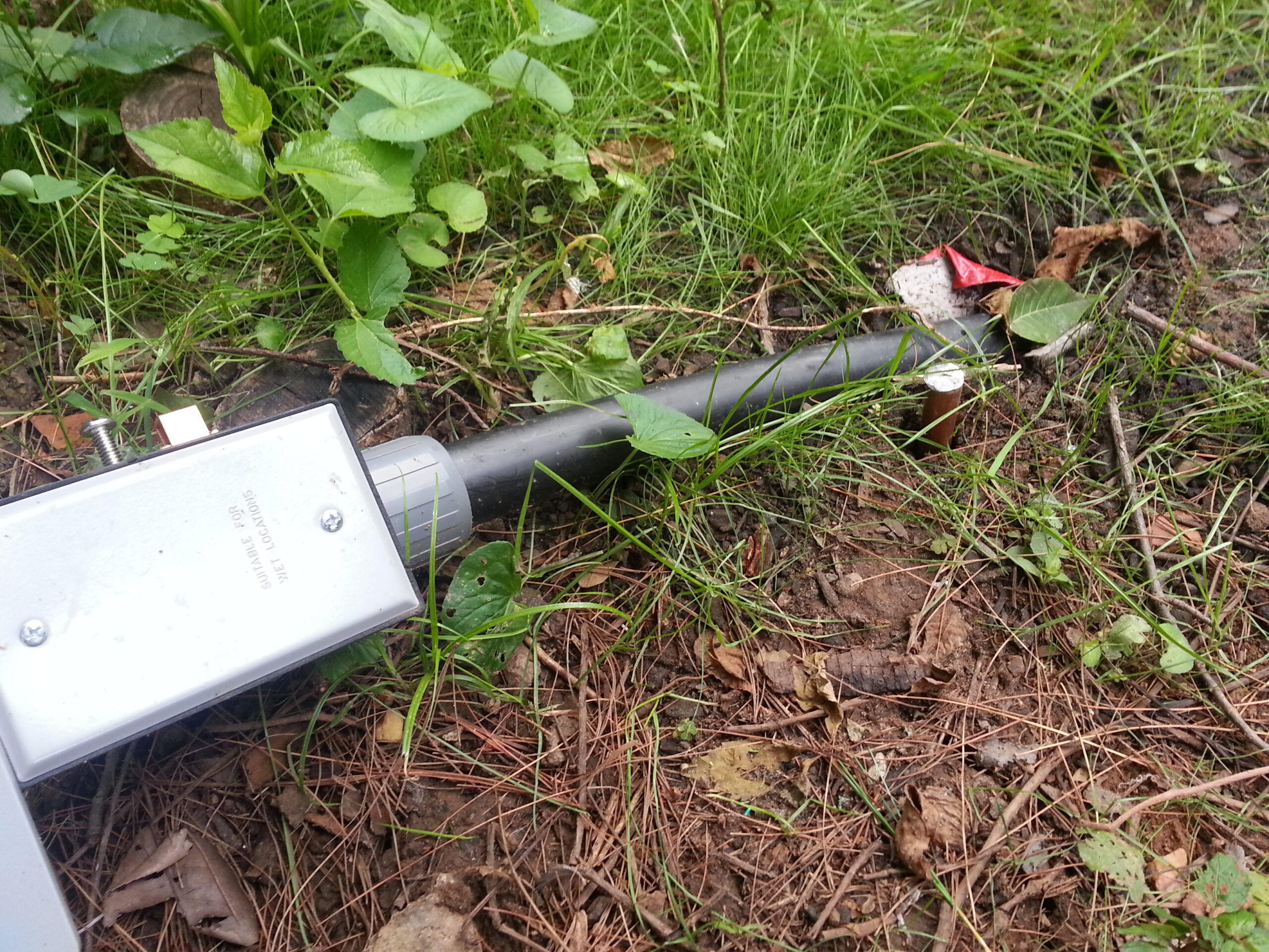
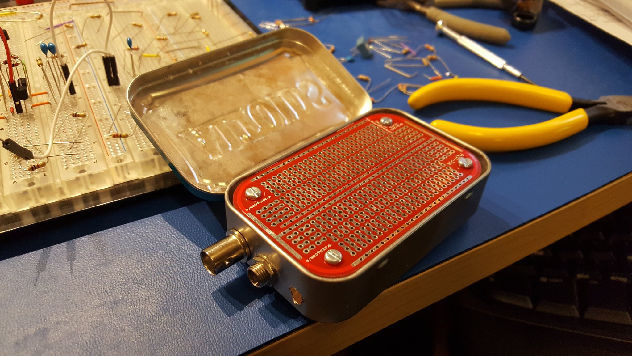
A while ago I discovered some prototyping boards that are designed to fit perfectly in Altoids tins. I purchased a bag of them and started collecting tins for little radio projects. I consider it a good idea to put anything that makes or consumes RF into a metal box — and this seemed like a good fit.

To begin, dry fit the big parts into the tin. If they fit, it’s time to build.
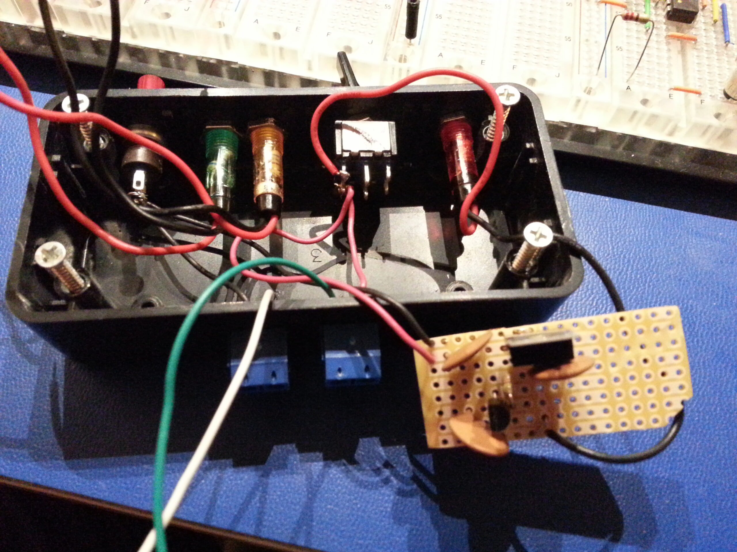
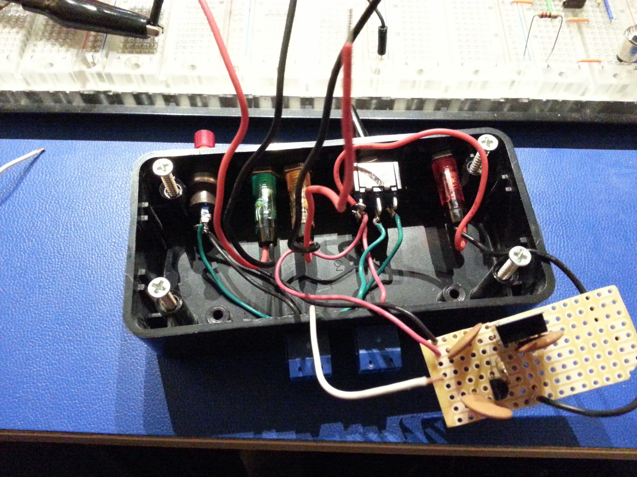
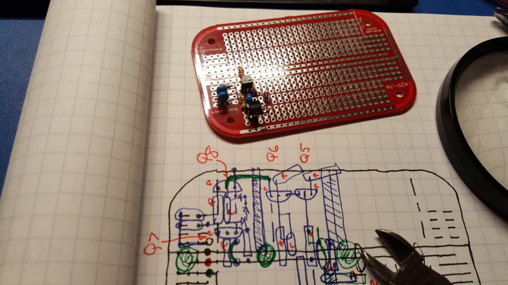
I had my lab tech carefully drill some holes and mount a BNC connector, barrel connector (for power), and stand-offs for the circuit board. Seeing that all of that fit nicely it was time to start building.
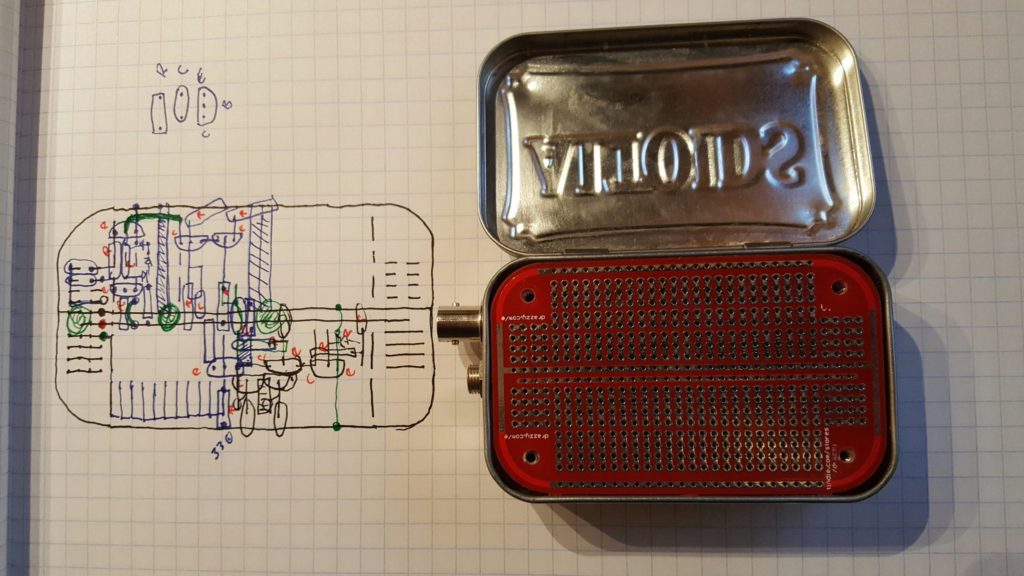
These things never go exactly as you expect, but to get a good result you have to start with a plan and evolve from there.
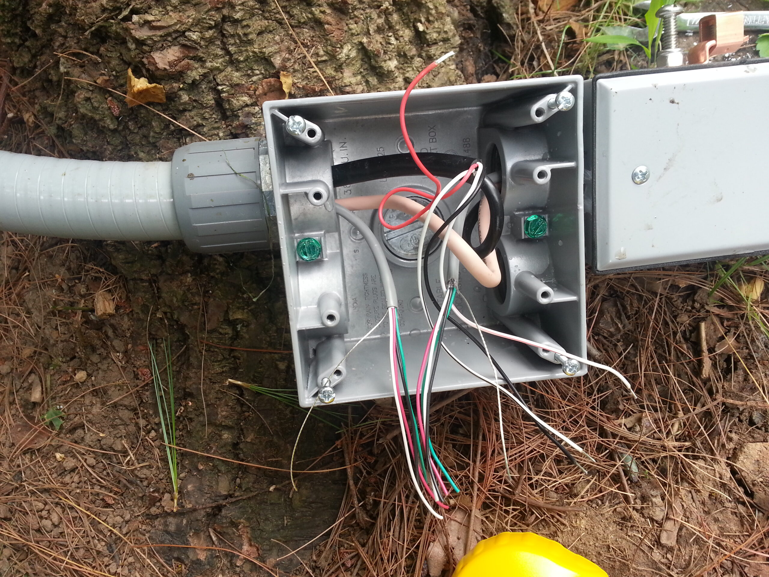
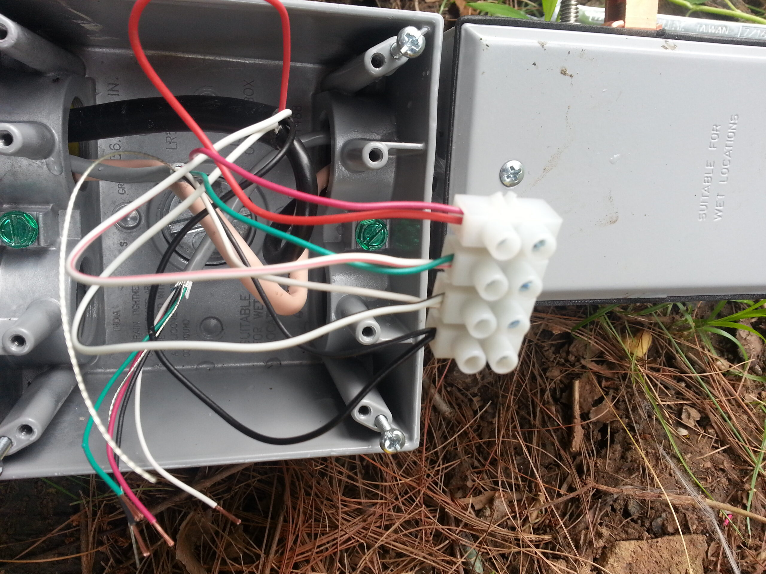
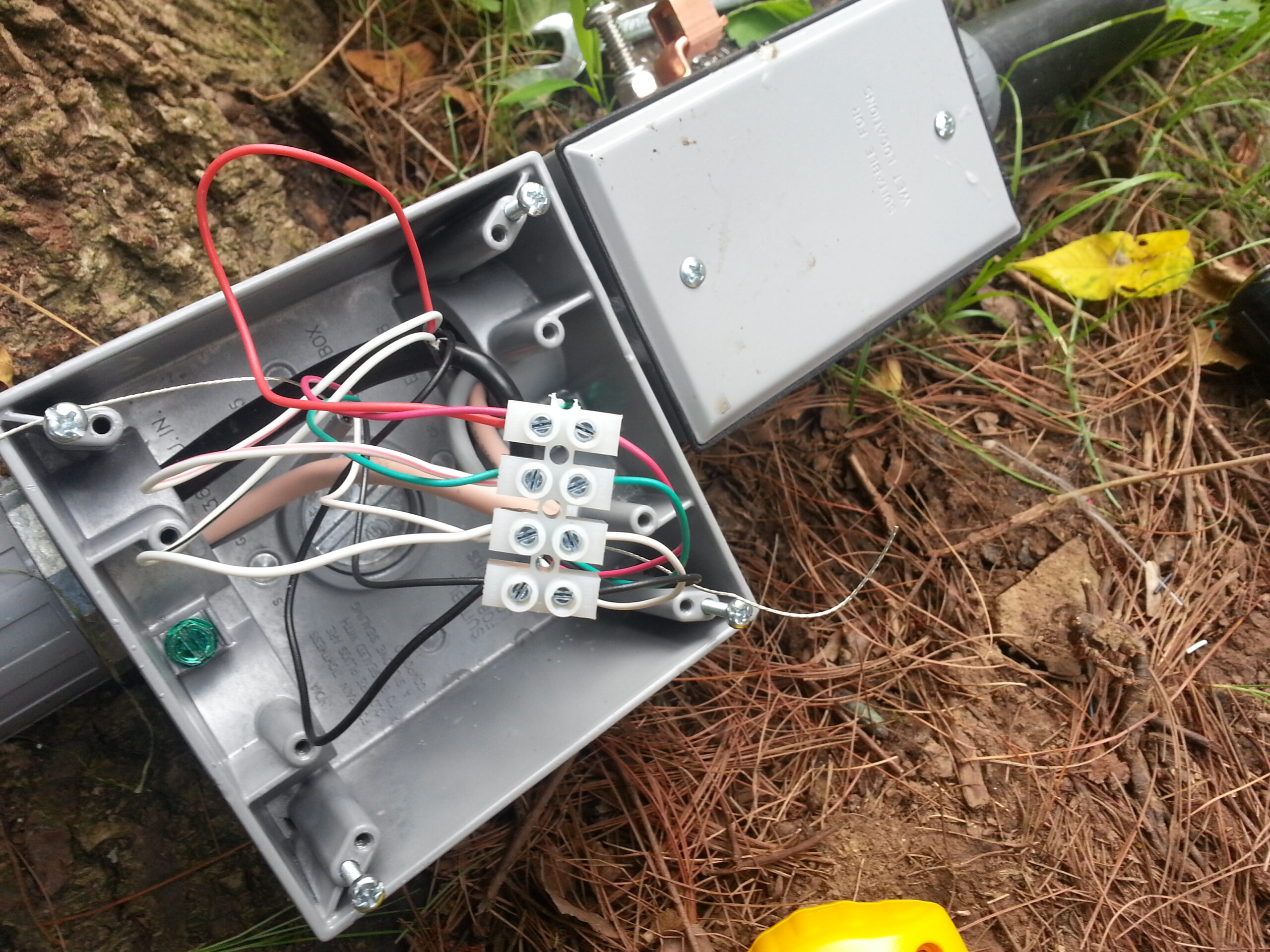
This device has a lot of potential challenges that most prototype projects don’t. For one thing we’re working with RF. I know, some will scoff and say that RF doesn’t happen until you’re well into GHz, but even at 10-50MHz the details matter. For example, there is a good deal of amplification going on here so we want to keep the inputs away from the outputs. We also want to be sure that grounding is handled properly; and we want to keep lead lengths as short as possible.
At the same time, we want to be sure the layout is beautiful — we’re making art!
All joking aside, if it looks good it is far more likely to work well… there really is something to be said for beauty. It turns out to be a fantastic short-hand for good engineering.
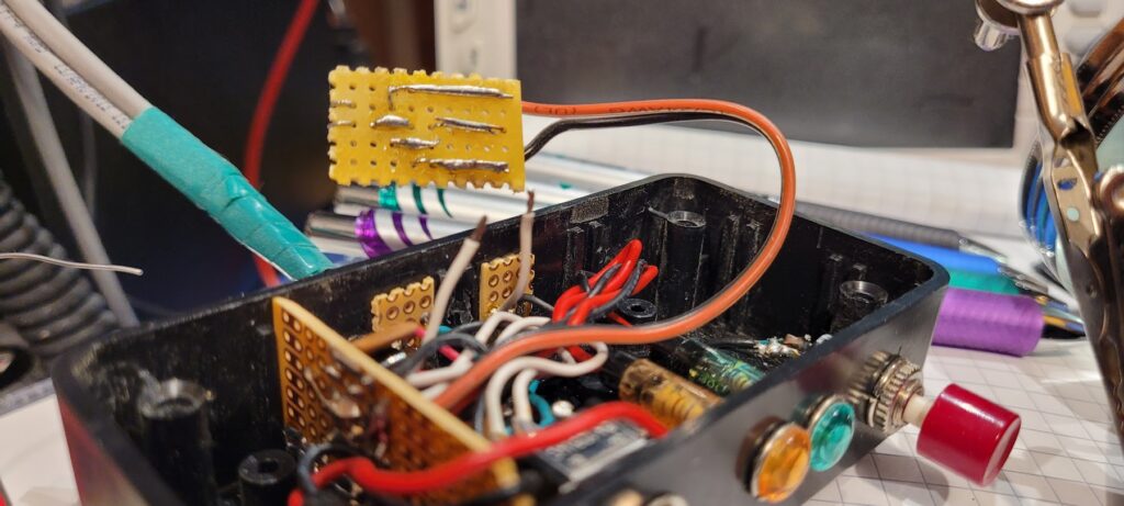
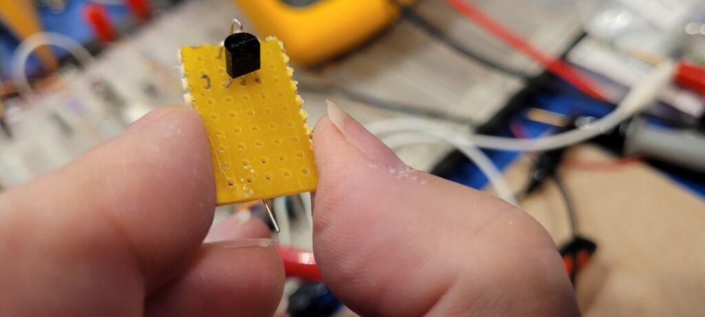
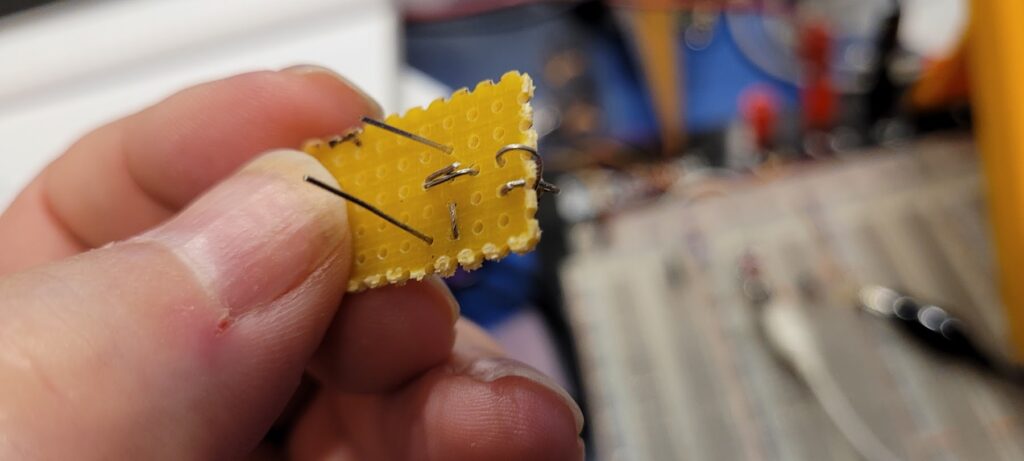
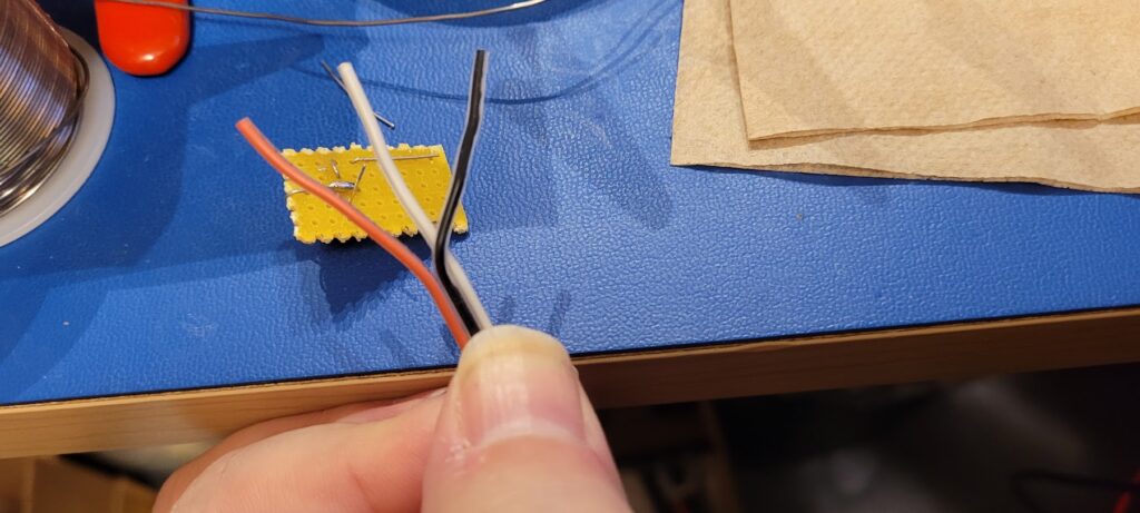
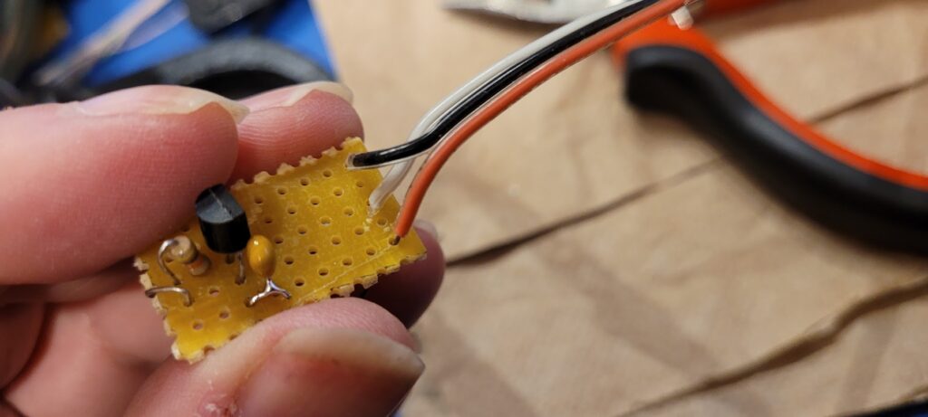
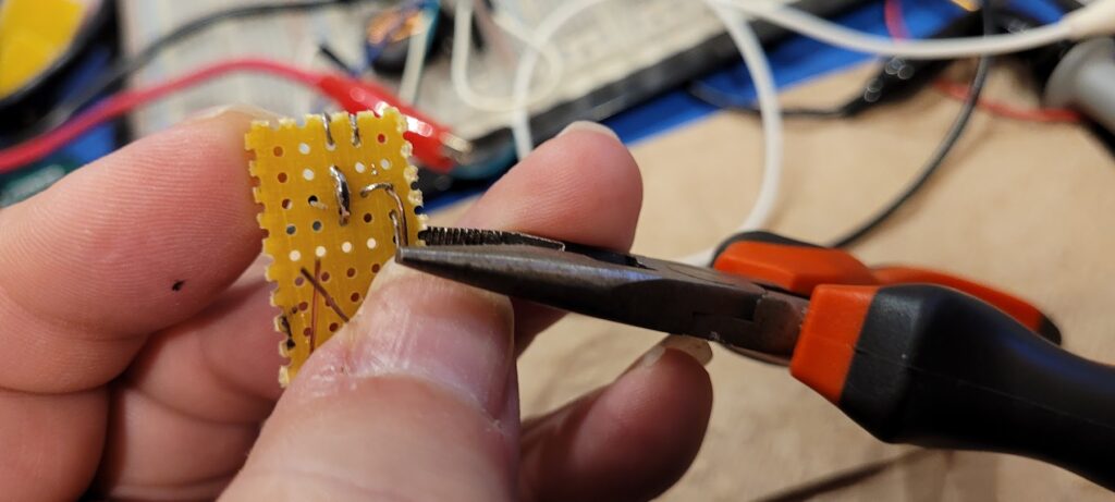
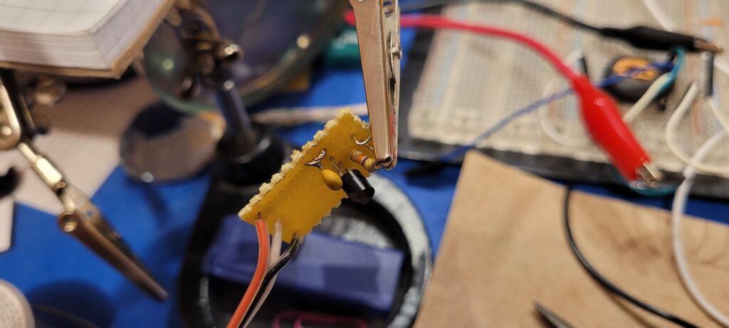
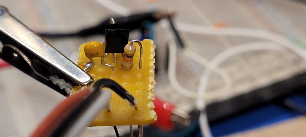
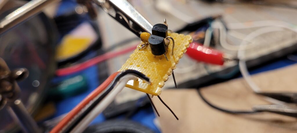
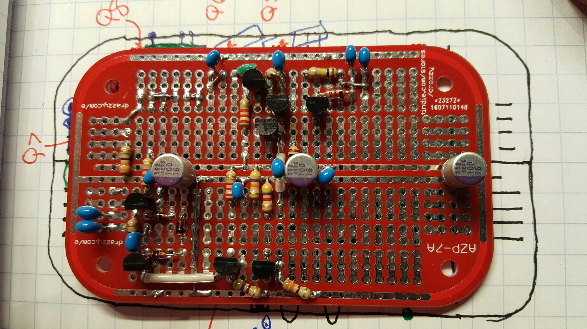
Once the basic plan looks good and all of the components have been accounted for it’s time to start populating the board.

Sometimes prototyping presents challenges that production won’t. Each regime informs the other.
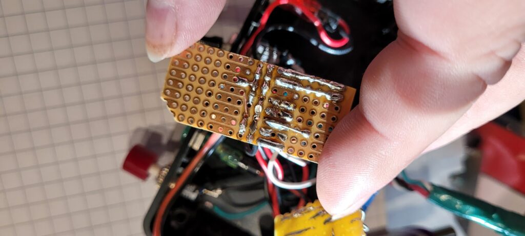
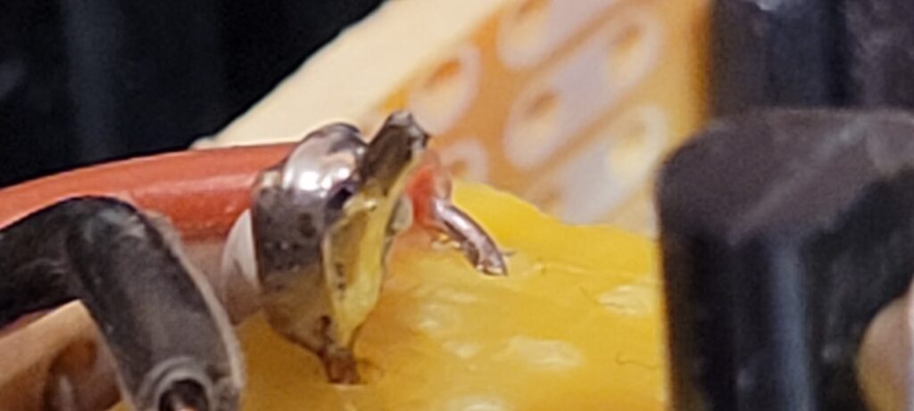
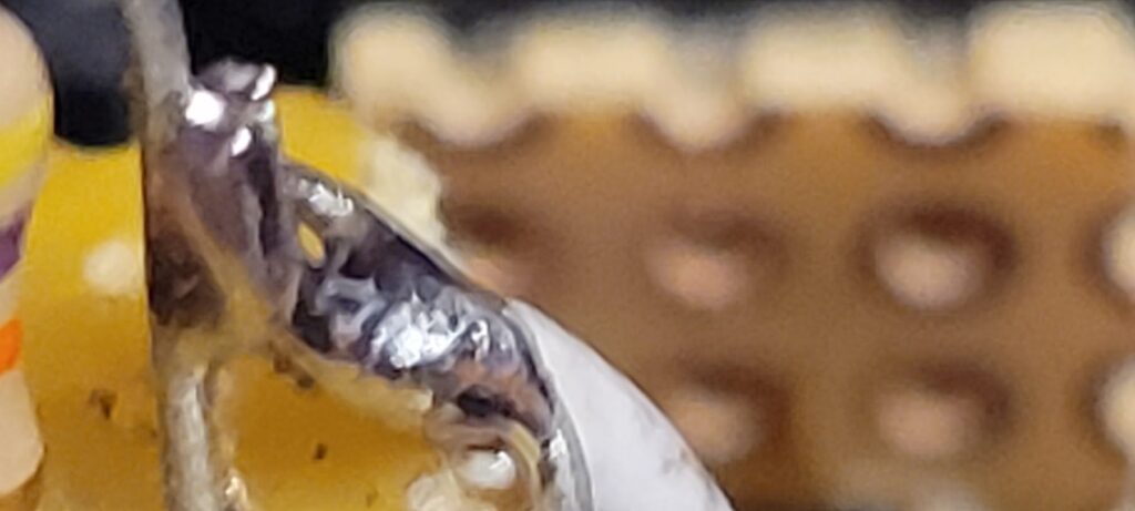
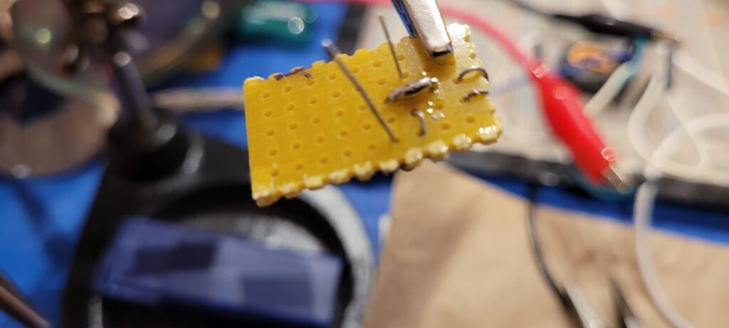
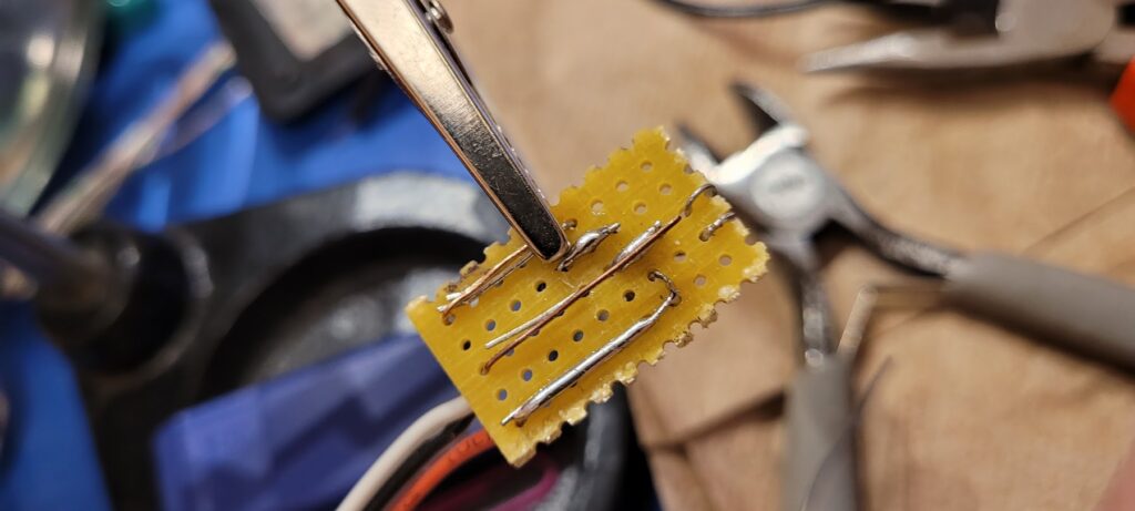
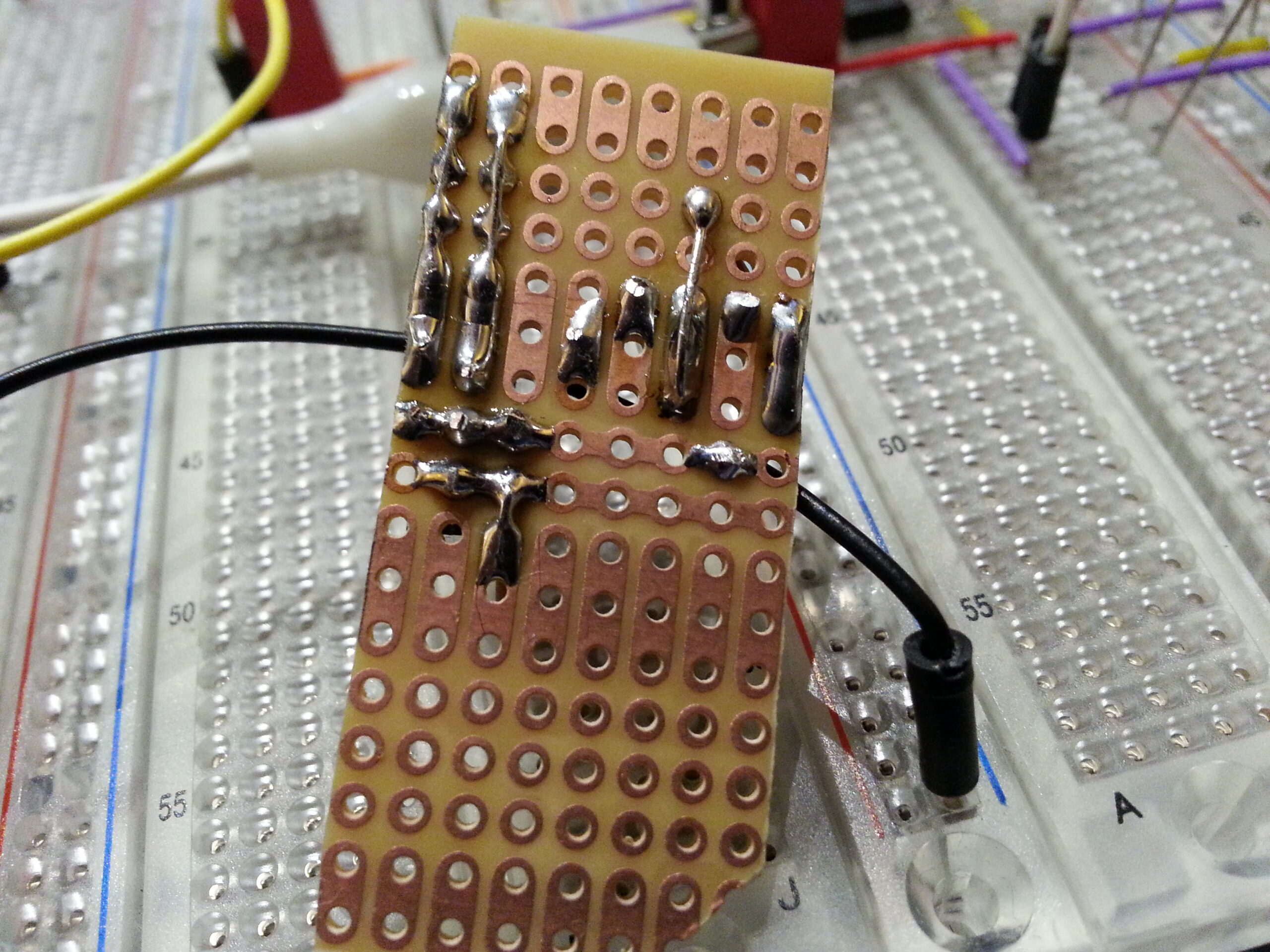
Right away I noticed a problem. These PCBs are fantastic — each hole is a via and the opposite side of the board has a matching trace. This makes it very easy to populate both sides of the board if that’s useful. But it also creates a problem that won’t happen in a production PCB. The cans on the aluminum electrolytics will short out the traces if they are allowed to touch the board!! So, they need stand-offs.
We can make stand-offs for the electrolytics by borrowing short pieces of insulation from some hookup wire. The insulation also helps remind us of the polarity.
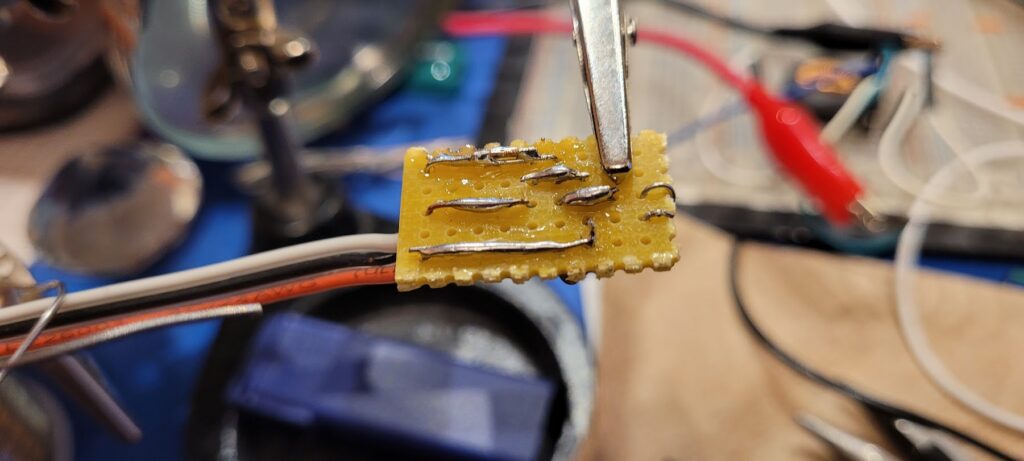
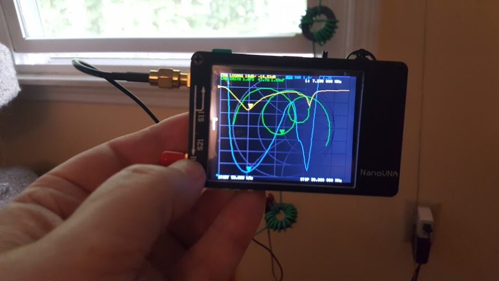
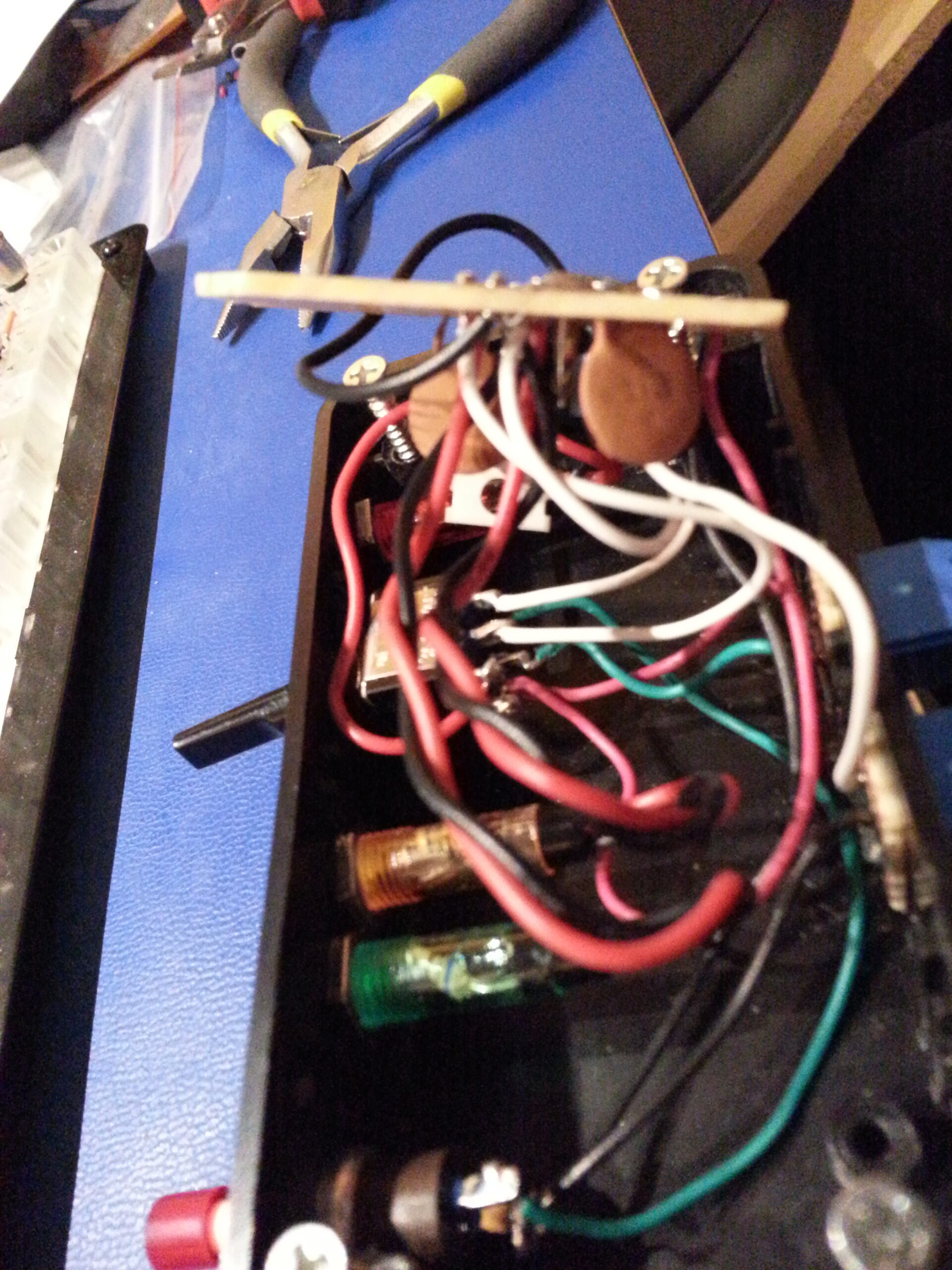
Each time a stage is completed it’s good to take a break, do some testing, and reflect on how the process is going and how well the build matches the plan.
I started with the power stage and decided to work backward from there. As usual I found myself making small adjustments to the plan as the build evolved. This is an important part of the process. Each time a change is made it’s important to look forward to the next steps and work through the rest of the build mentally. It’s a learning process; and it’s not unusual to discover that significant changes should or must be made. The goal is to see these well before you get to them so that your build doesn’t grind to a halt with some impossible problem. It’s always better to rework a design before parts are on the board than it is to force a bad layout and bodge your way around a physical impasse. Take the time to look ahead — it’s always worth it. The lessons you learn will inform your production planning if the prototype ever turns into a product; and your skills and intuition will dramatically improve with the practice.

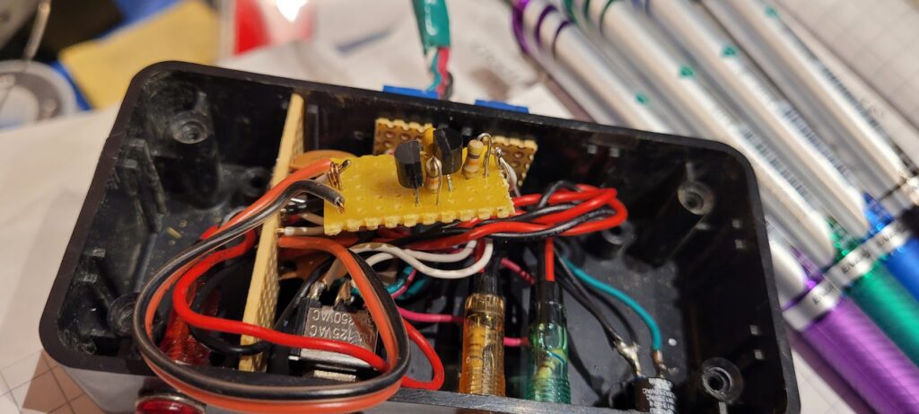
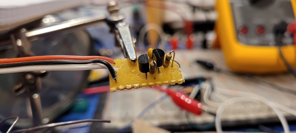
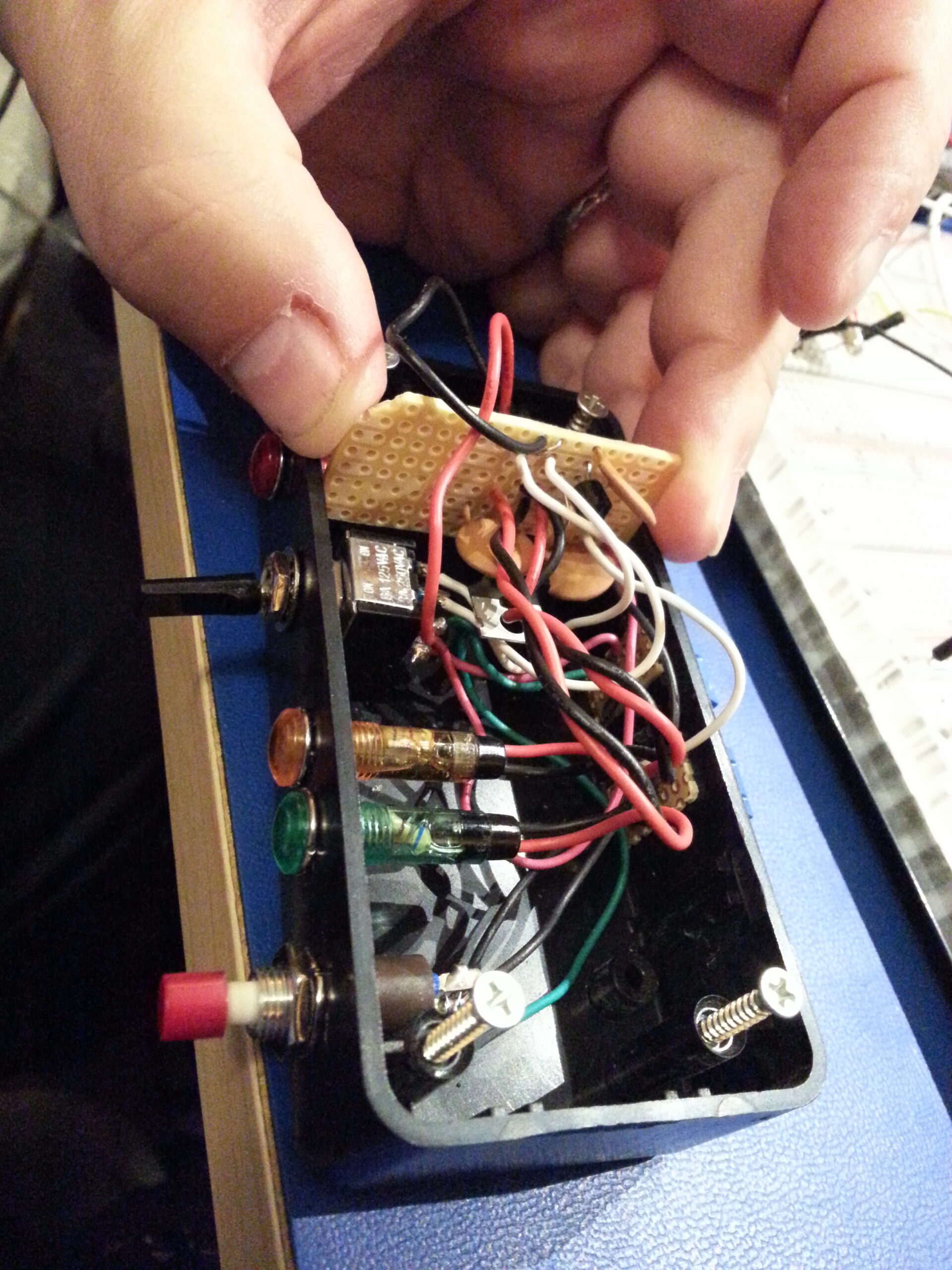
Once all of the parts are in place it should look like a work of art. If it looks good chances are great that it’s performance will also be good.
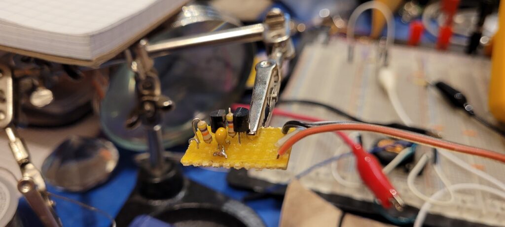
You can’t always get a prototype to look like a production board; but the final build should have a lot of the same qualities. The signal routing should be intuitive and efficient. Parts should be straight, neat, and laid out logically. Leads should be short. Jumpers should be short, few and tidy. If you buzzed out your circuitry as you completed each section you should be ready to apply power. Smoke Test!
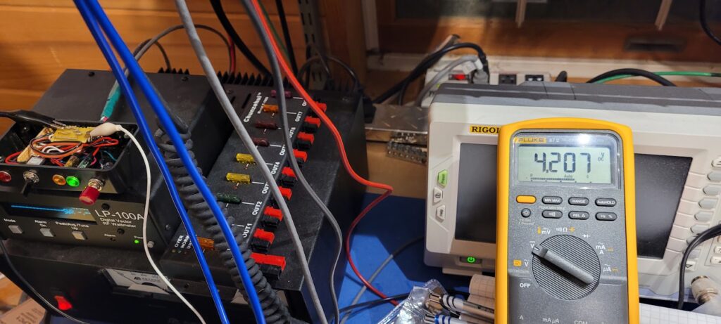
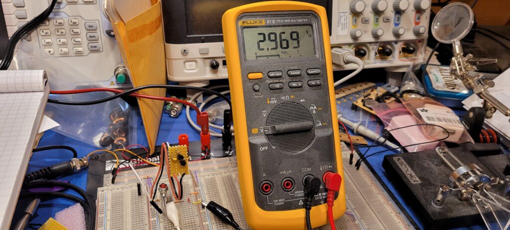
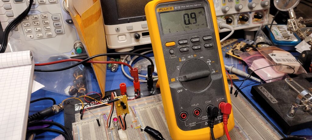
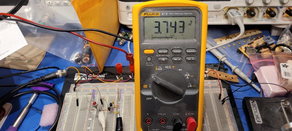
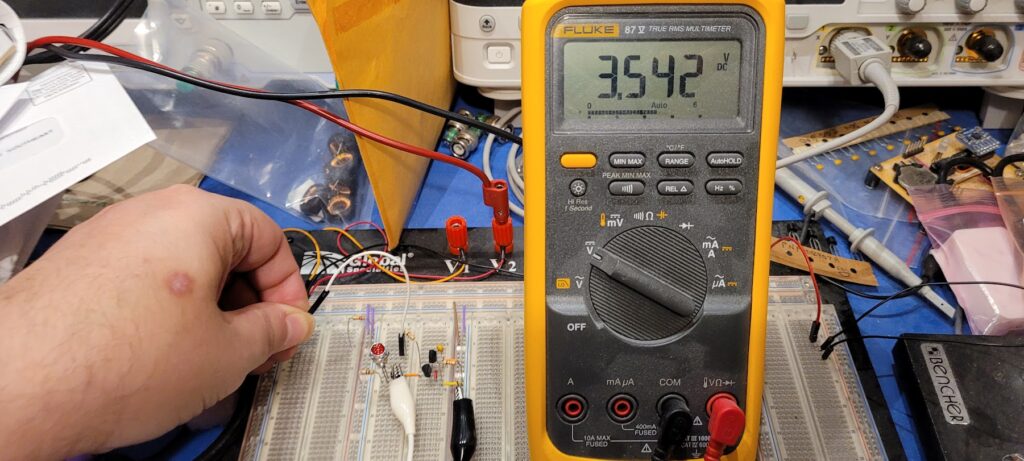
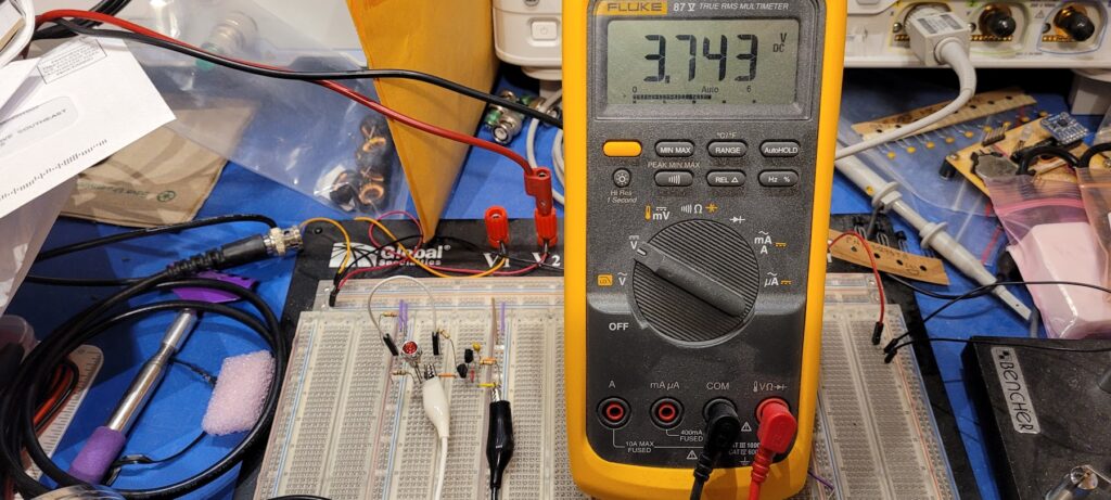
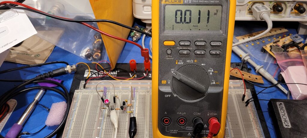
The Smoke Test — Apply power (and signals) and verify no magic smoke escapes. You did test all of this multiple times getting to this point… right?
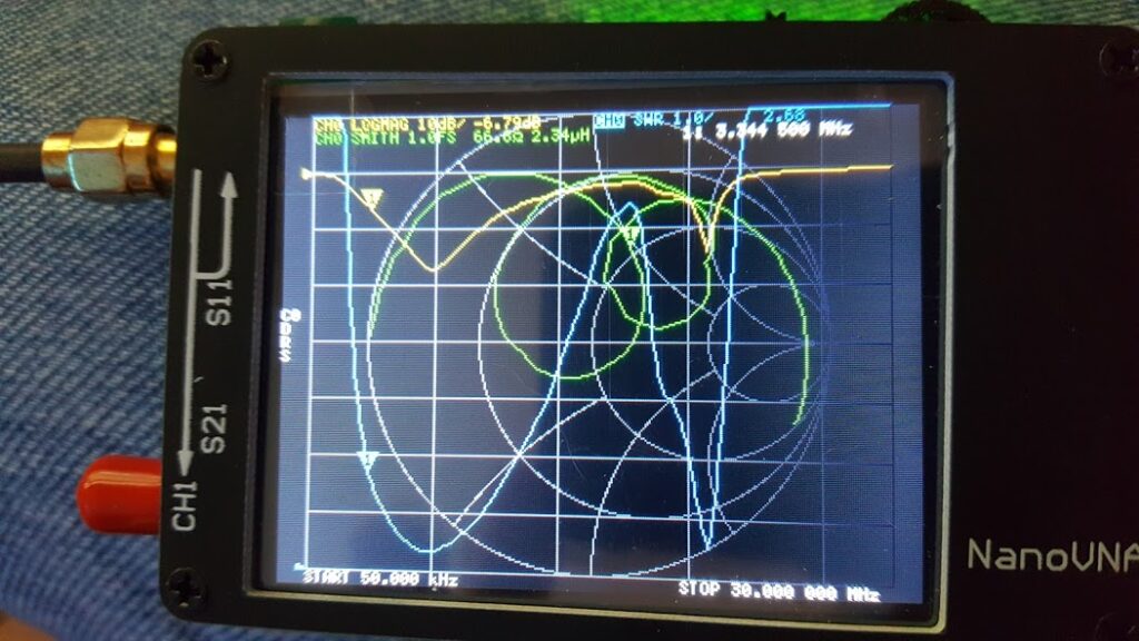
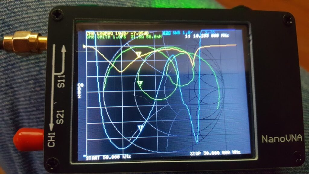
I built the prototype by pulling parts directly out of the breadboard for each section as I completed it. In theory, this means that I have exactly the same circuit in my prototype as I had tested on the breadboard. It turns out that this never works exactly like you expect. In this case, I’ve got good results that are very close to those I had on the breadboard but inexplicably there are minor differences. For one, the output voltage is ever so slightly lower than it was on the breadboard. That’s odd — because the conventional wisdom is that what you build on a breadboard will generally perform a bit worse than what you build on a PCB (or other construction). This is especially supposed to be true of RF circuitry.
In the end every build is a little different – and that’s to be expected based on my experience. What matters is that the magic smoke stays well contained and that the circuit performs substantially as designed and previously observed. If it’s close it’s probably right — but make some comparative measurements to be sure.
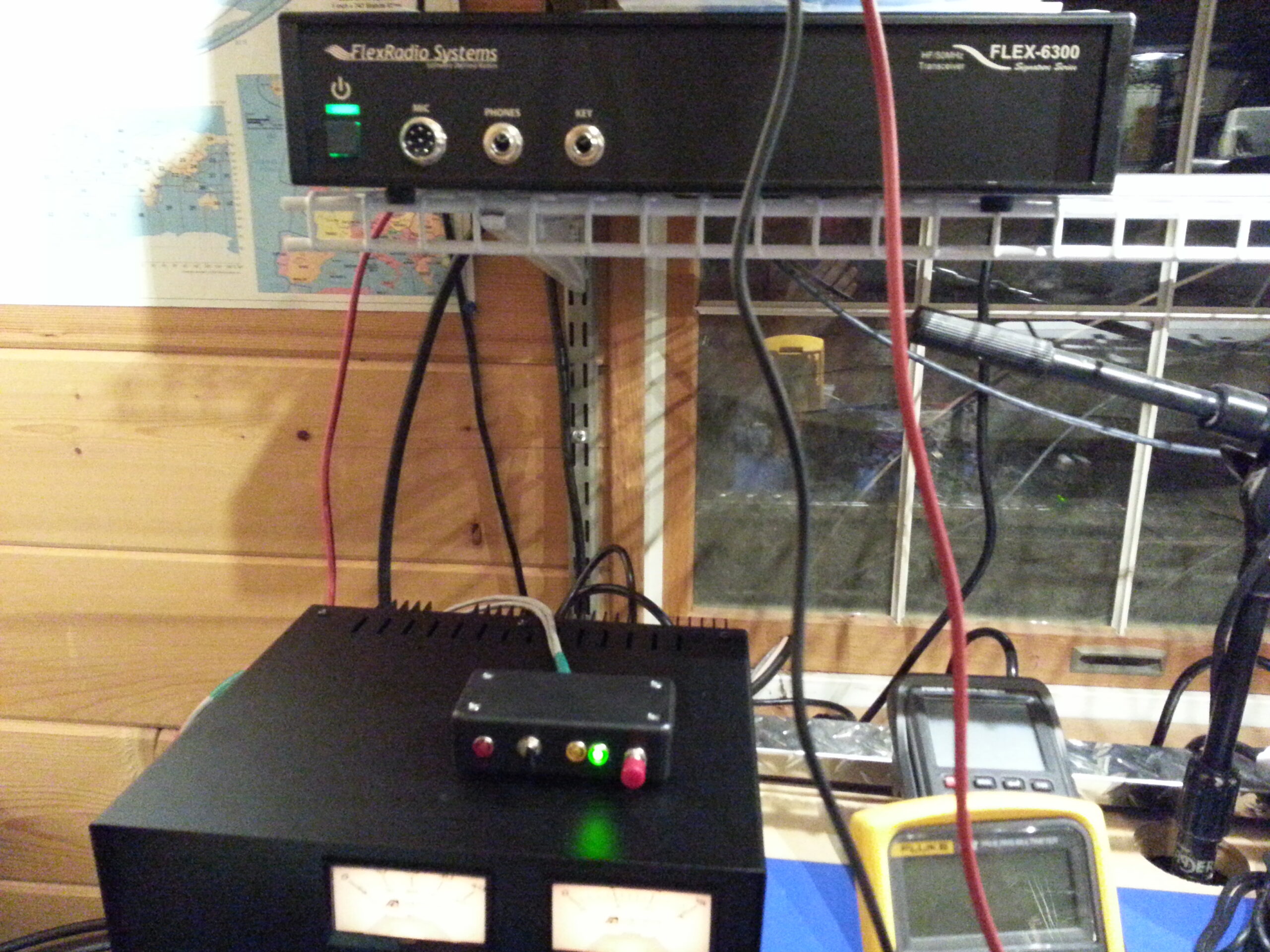
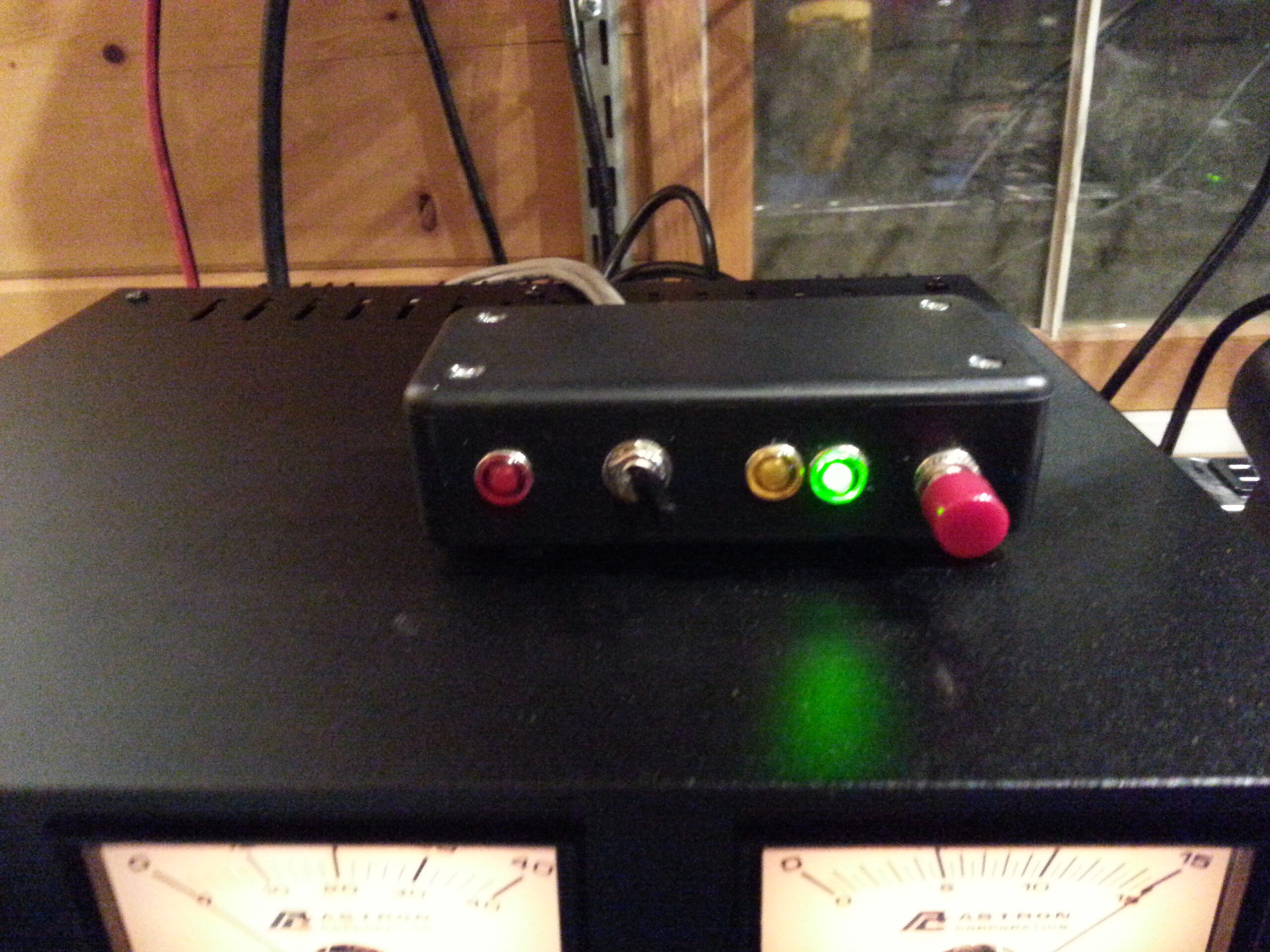
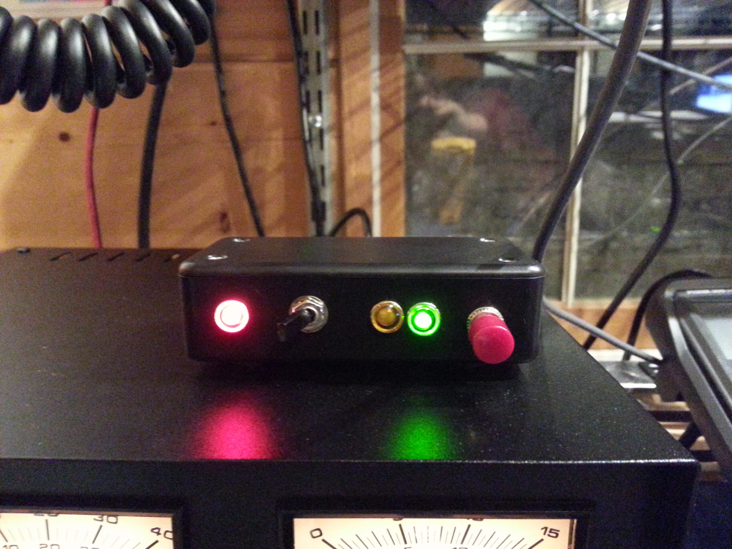
When all of that is done and it looks right it’s time to put it in the box and do the final testing.
Next Steps
I am still considering possible improvements to this project as well as some projects that are inspired by it. One of the first things I’m likely to try is adding a small bypass cap to Q5 to ramp up it’s gain with frequency. If this or some other frequency shaping can be done linearly then I might consider going further and changing the gain structure to see how close to a truly flat response spectra it can produce.
I also have some ideas about exploring some of the other waveforms that emerged from this project and some other techniques. One that I might try involves using an ATTiny85 along with some of my encryption / prng algorithms to generate white noise with specific waveform characteristics, possibly even by modulating the output of the noise generator found here.
Another technique I might explore would possibly use some plain old 74HC00 logic to build hardware versions of LFSR based PRNGs and drive that logic with the noise generator from this circuit to see if that can be made to produce truly random data with well formed digital characteristics. There are a lot of areas to explore… FPGAs perhaps?
Noise, chaos, and randomness are very interesting topics with rich opportunities for further research.
If you build one of these or something similar please let me know how it goes.
If you have ideas about this build I’d love to hear those too.