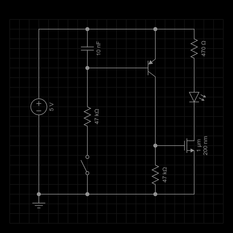
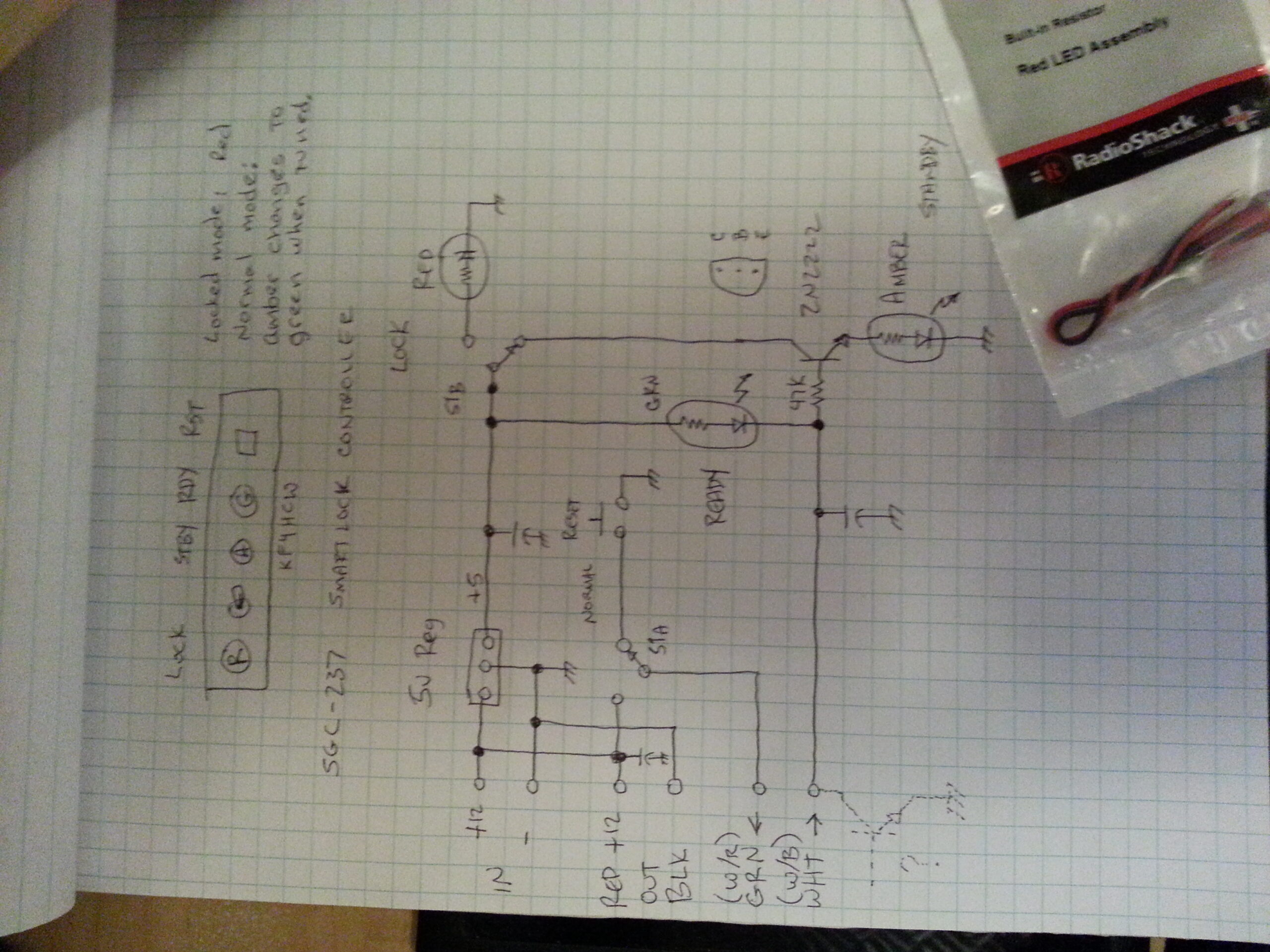
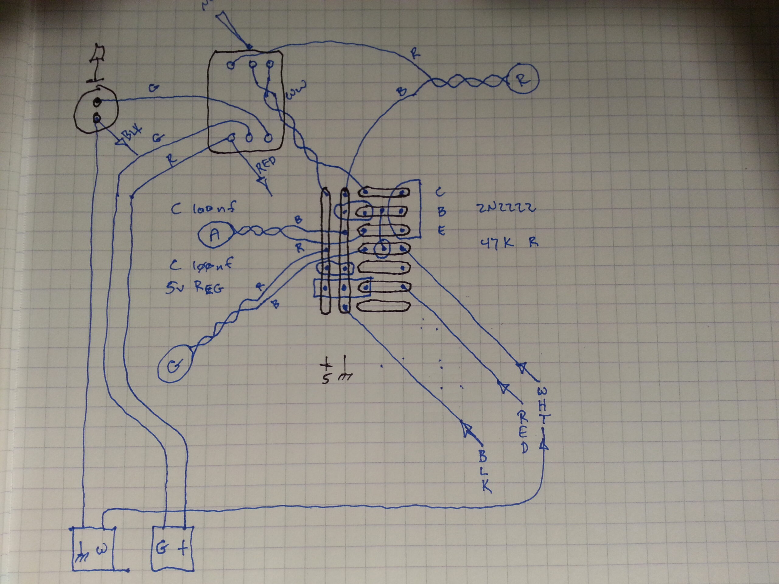
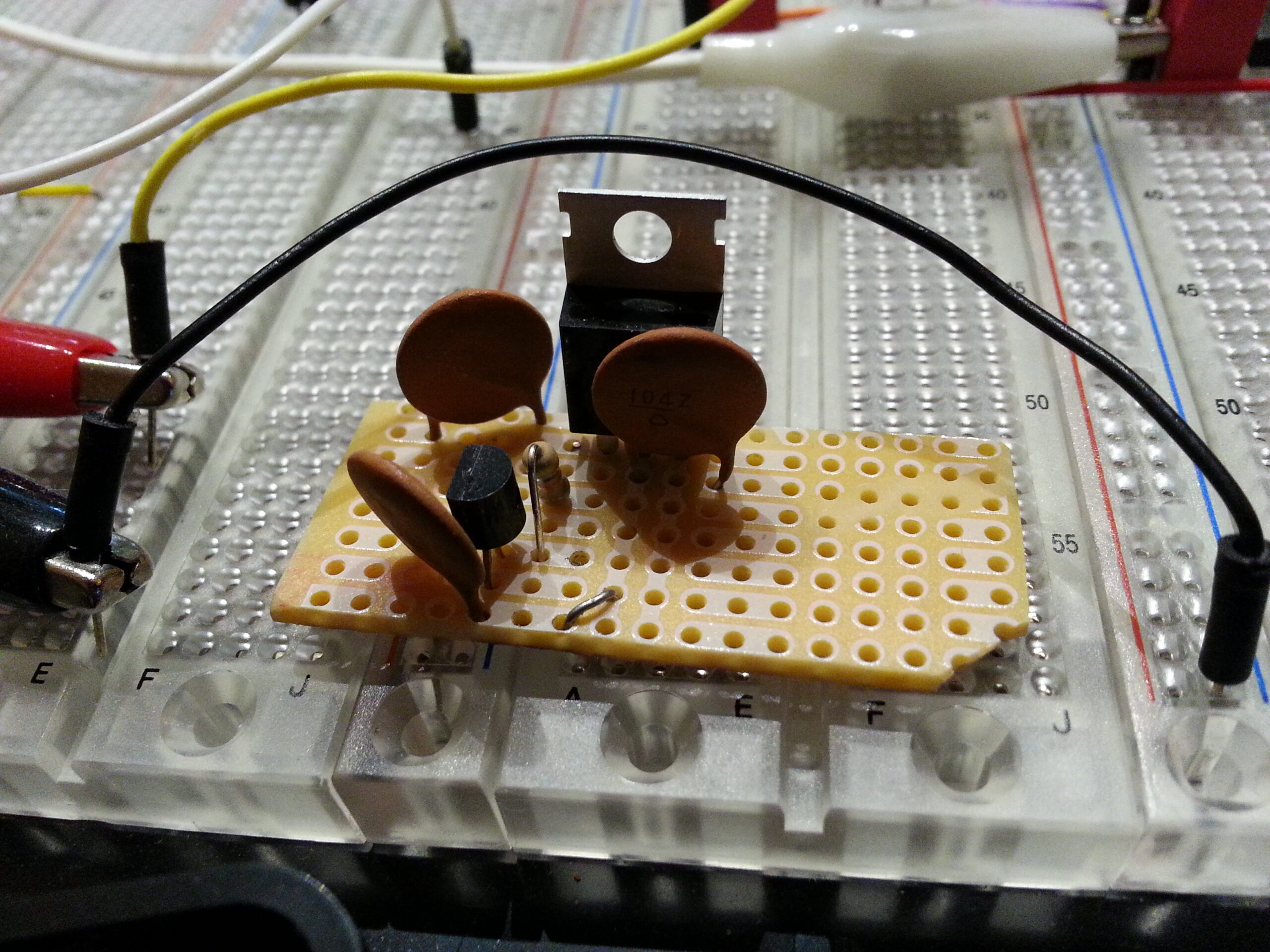
Sense Wire Loop
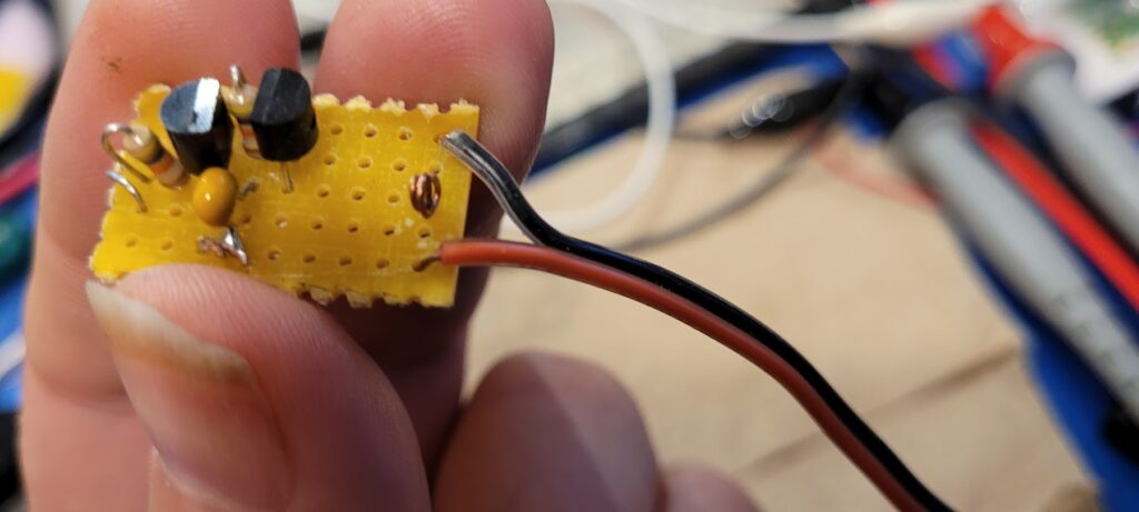
The first step to prepping for installation is to clip the sense wire used for testing and convert it into a loop – to act as a terminal on the board. The plan is to clip the existing sense wire in the controller and insert “sketchy” into that line. In order to make that work we need to have an easy way to connect both ends of the clipped sense wire. A loop on each end of the board will do nicely.
Find Power
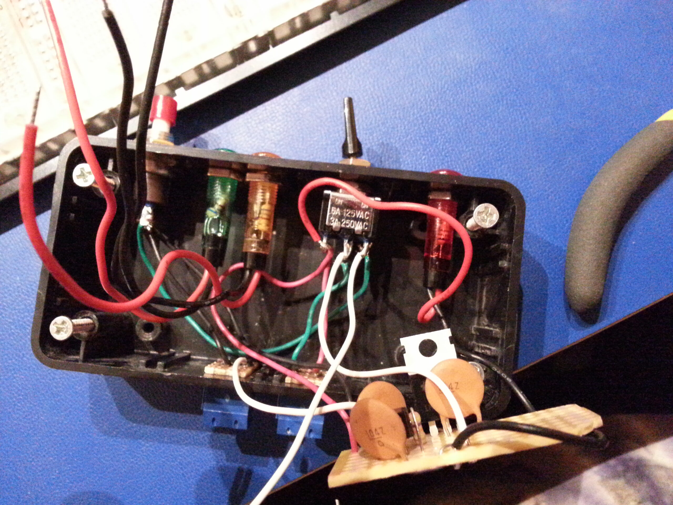
The next step will be to identify the cleanest way to get power to our board. As it turns out the controller has regulated 5V rails in the middle of it’s board AND (lucky for us) there are two adjacent holes on those rails exactly in the right place for our ribbon wire. Here you can see the red and black ribbon wire matched up with the rails… carefully inspecting the circuit to make sure the polarity is correct and precisely where these wires will come through the controller board.
Not visible in this shot, on the top side of the board near the top of this picture I identified the 5V regulator and it’s pins to make sure which of the two rails in the middle are positive and negative.
Power Leads Inserted Top Side
Here I’ve inserted the power leads from the amplifier into the controller. They fit correctly flush up against the board and it’s clear that the colors for + (red) and – (black) match up with other connections on the board. This is another good sign that I have the polarity right.
Power Leads Inserted Bottom Side
Viewed from the bottom side we can see the wires coming through the holes in the power rails on the controller. It all looks correct (again checking carefully) so we can solder it in.
Power Leads Soldered
Here is a close up inspection of the new connections soldered into the rails. No unwanted solder bridges. Nice smooth, shiny solder joints. Some of the other nearby joints leave holes uncovered but otherwise they look fine… so I resist the urge to reheat them.
No Melted Insulation Top Side
One of the reasons I resisted the urge to re-heat those other joints is because I don’t want to begin melting insulation or causing other trouble. The connections themselves are electrically just fine – -it doesn’t matter at all (except maybe aesthetically) if the holes aren’t completely filled in. But, it DOES matter if the insulation melts potentially causing a shorting hazard.
Here we can see that the newly installed wires to power “sketchy” are not melted at all. That means there was just enough heat for just long enough to make a good solder joint.
Clip Existing Sense Wire
Now that power is available to the amplifier board we need to put it in line with the sense wire. The existing sense wire is the white wire in the maw of the clippers. I have dry-fit the board into that location in the box and so I know I can clip the sense lead right in the middle of that location. One side of it will bend back to the input of the amplifier and the other side will bend back to the output. This will leave just enough extra lead to safely solder the connections and move the new board around to the right position in the box.
Carefully Calibrate Stripper
A tricky part of the installation will be trimming the insulation off of the freshly clipped sense wire. It’s important to get this right the first time… because if this step goes wrong then there will be a lot more work to do replacing that wire and it’s other connections.
The wire strippers have a small bolt and nut that can be slid into the correct position to calibrate the strippers and then tightened down. So, with the calibration bolt loosened, I take a similar wire that I can use as a gauge and carefully close the strippers on it until they just barely cut all of the insulation without nicking the conductor. Then I carefully tighten the bolt and re-check that the calibration didn’t move during that process. It seems like a lot of work – but sometimes there is no substitute and I “really” don’t want to have to replace those wires if I can avoid it so it’s worth the effort.
To make sure I have it right, I strip a few more bits of insulation off of the test wire and inspect the conductor to ensure it’s not nicked; all the while making note of the pressure required to squeeze and pull the insulation so I know what will feel right when I do the real thing.
Sense Lead Cut, Stripped, and Tinned
Once I’ve stripped off about half a centimeter of insulation from both halves of the sense wire I tin the ends so that it will be easy to get these soldered into place. With tinned wires, one can push them through the connector loops and give them a quick hit with the soldering iron to get them connected. Then when both are done it’s easy to go back and re-heat them and fill them in a bit without having to worry much about the board or connections moving around during the process.
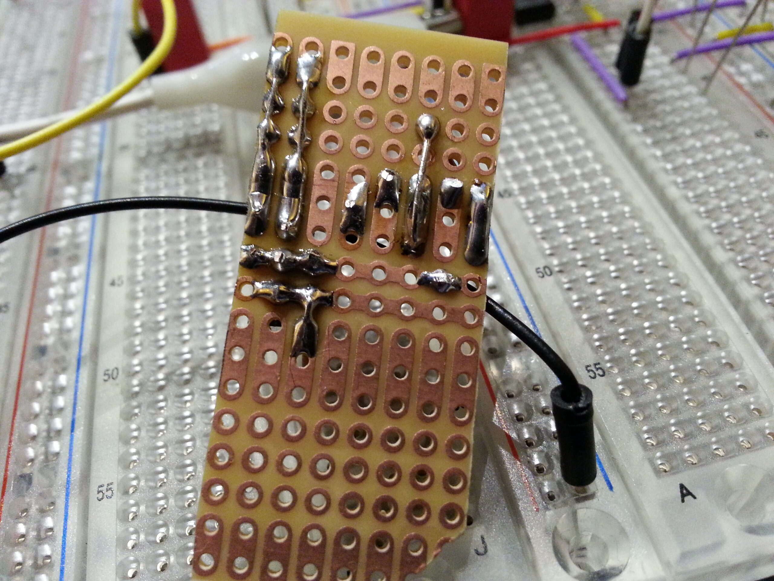
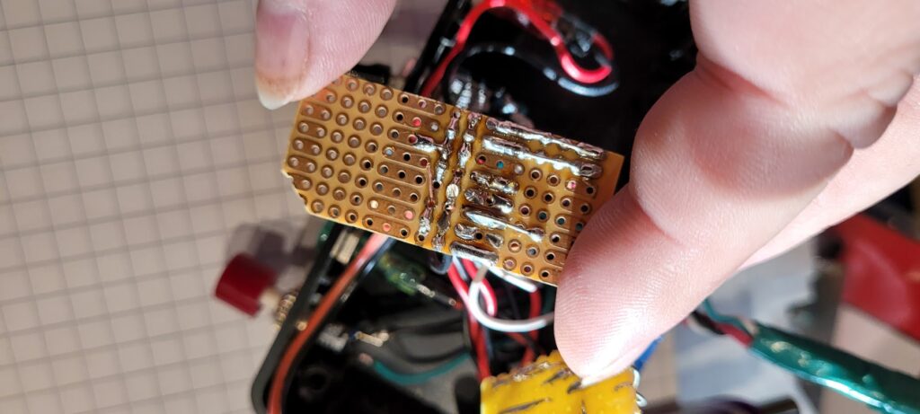
Sense Leads Inserted Into Loops
Here is a shot of the board in place, top-side up, with both ends of the sense wires “tacked” in place.
Sense Leads Soldered
With that done, we can go back and re-heat the connections and fill them in a bit to make things good and solid. Here is a shot of that from the top at about the angle I saw soldering them.
Side View
Here is a shot more from the side.
Sense Lead Output Close Insepection
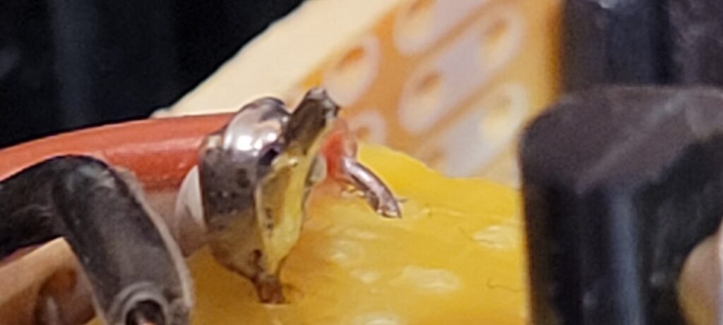
Just to make sure the connections are solid I used the camera to take close-up inspection shots — here is the output lead close up.
Sense Lead Input Close Inspection
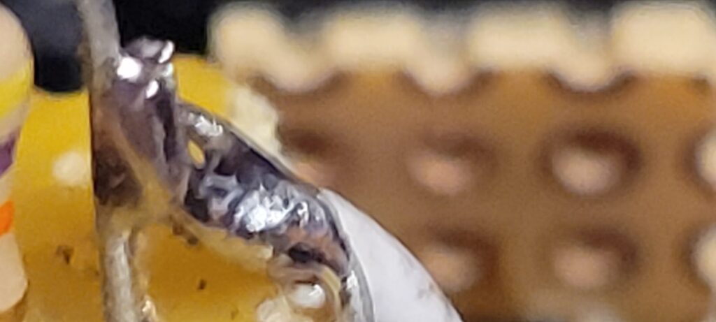
Here is the input lead close up. This shot is a bit motion-blurred, but it’s clear that the connection is solid and shiny.
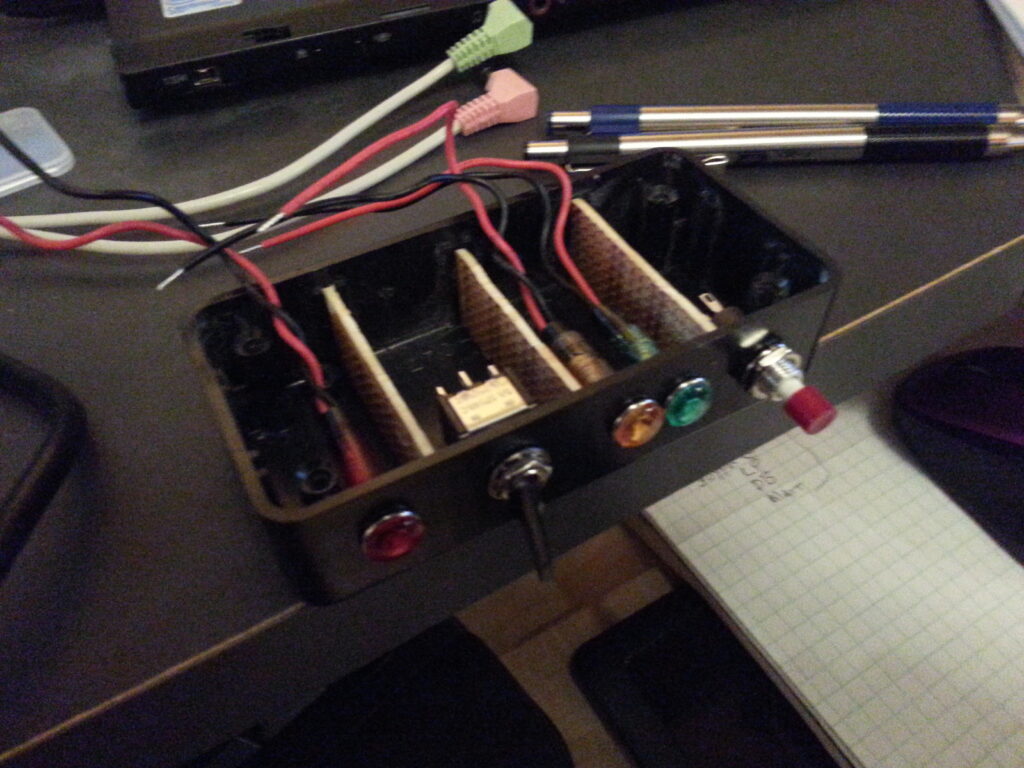
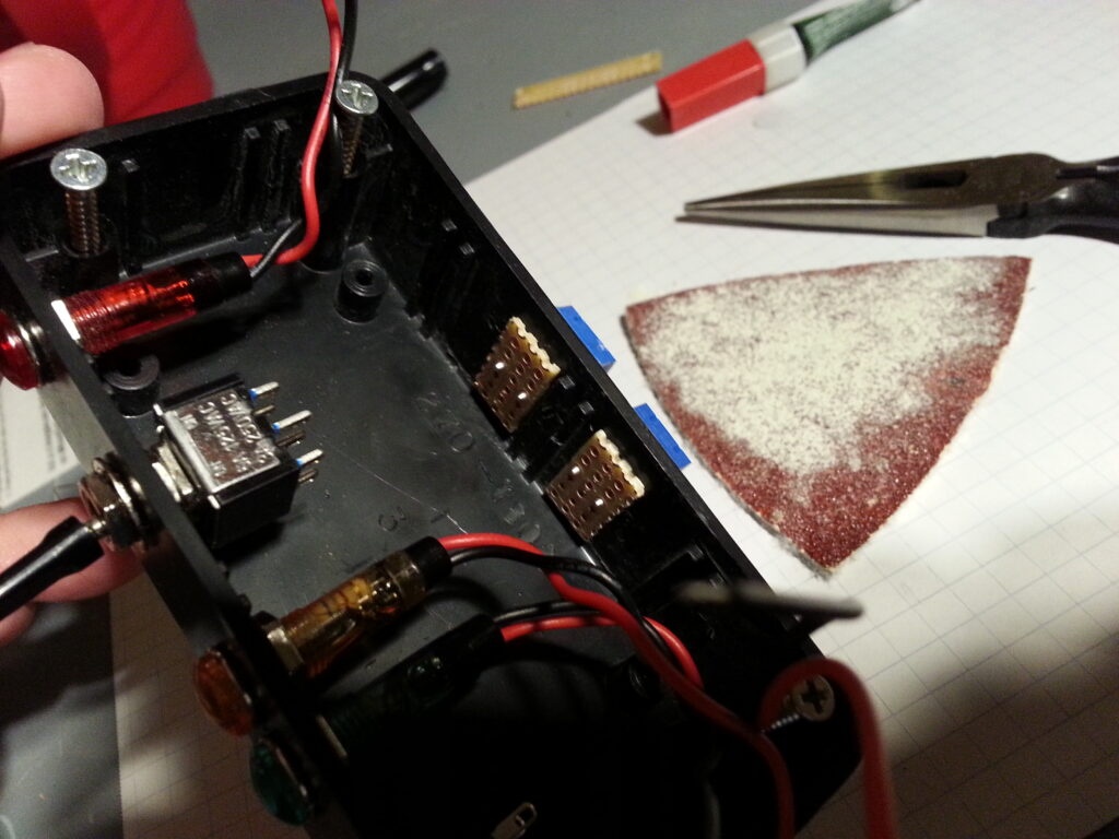
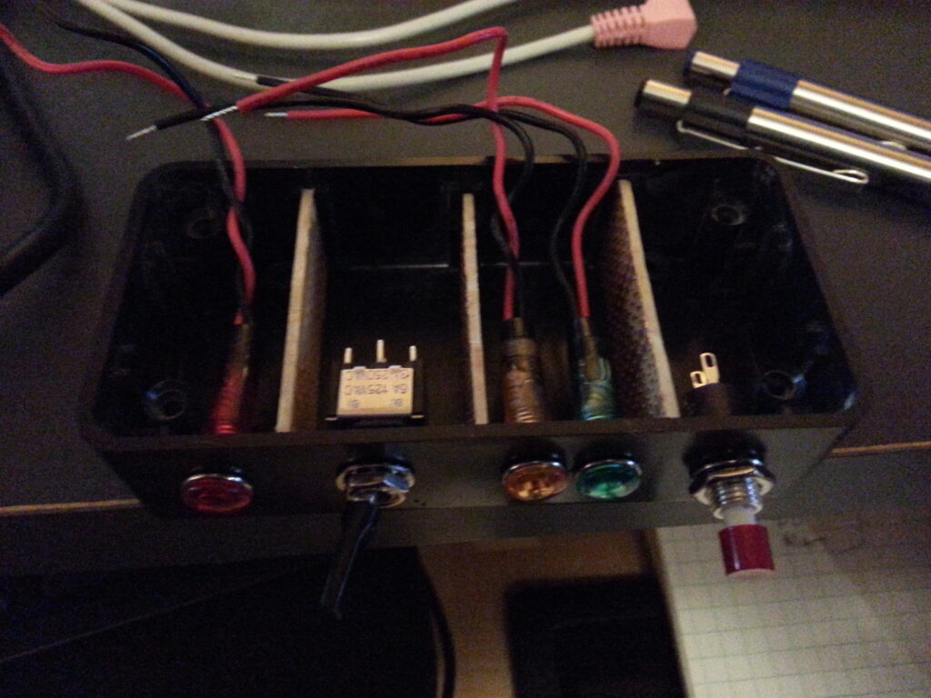
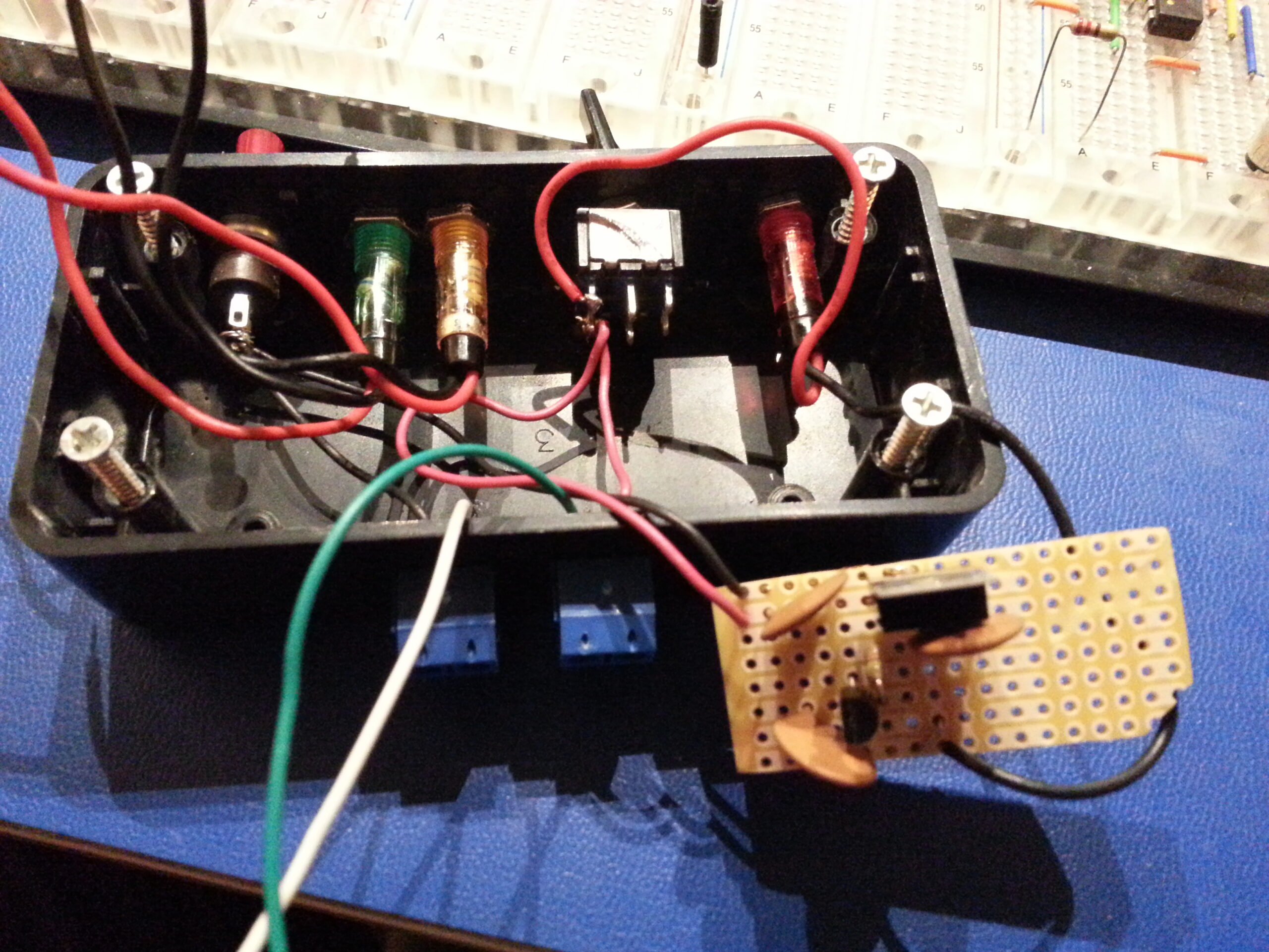
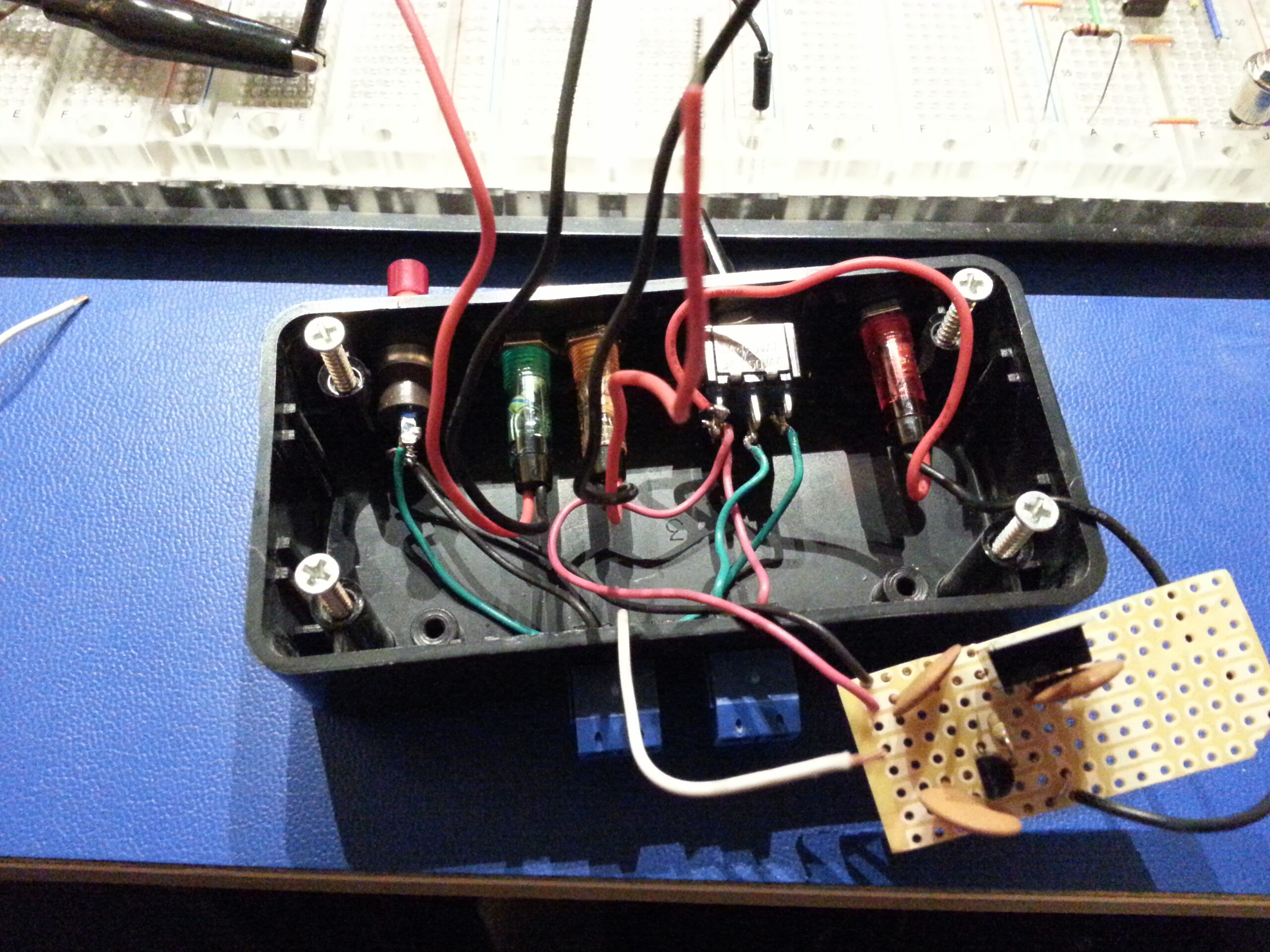
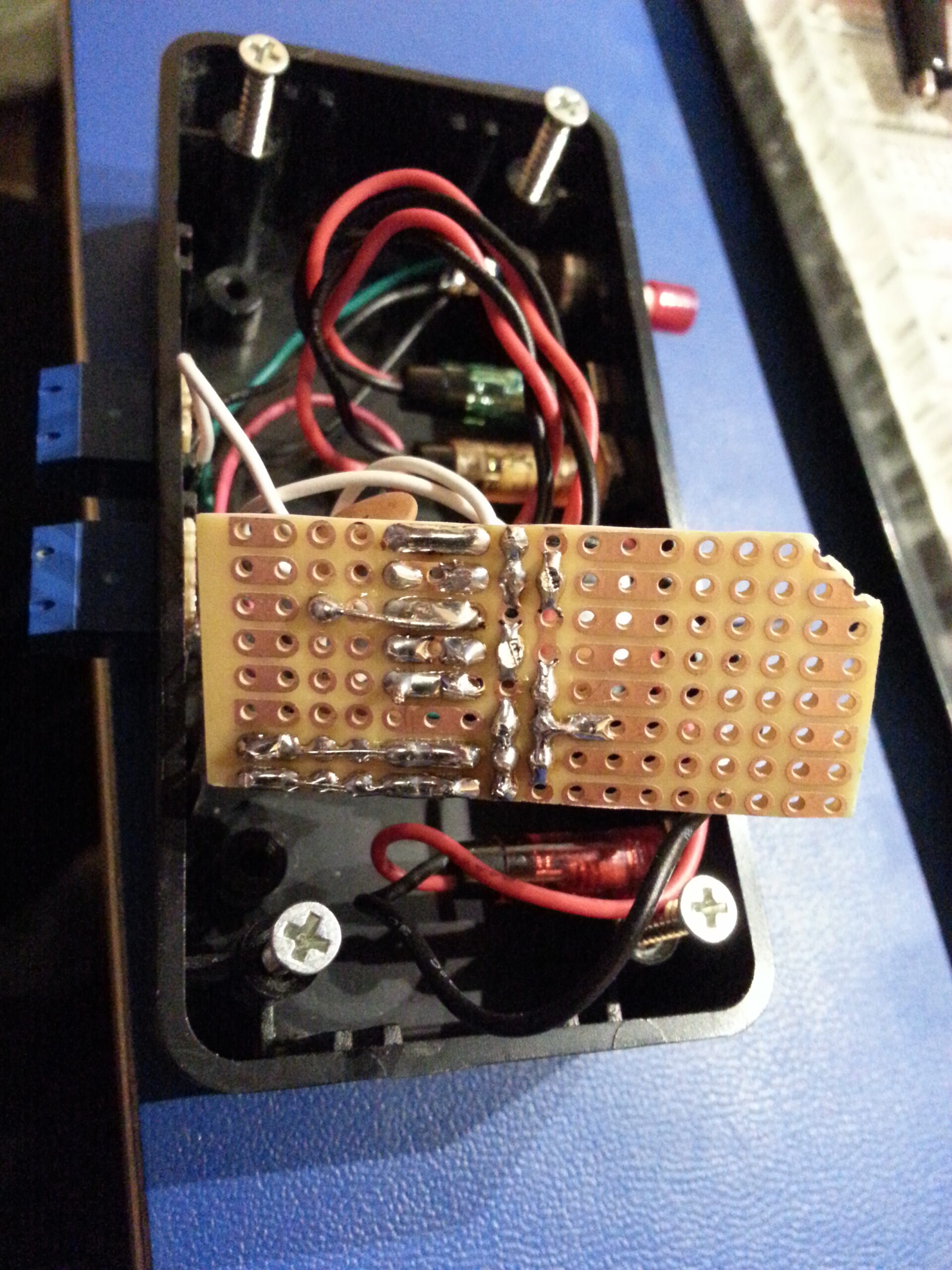
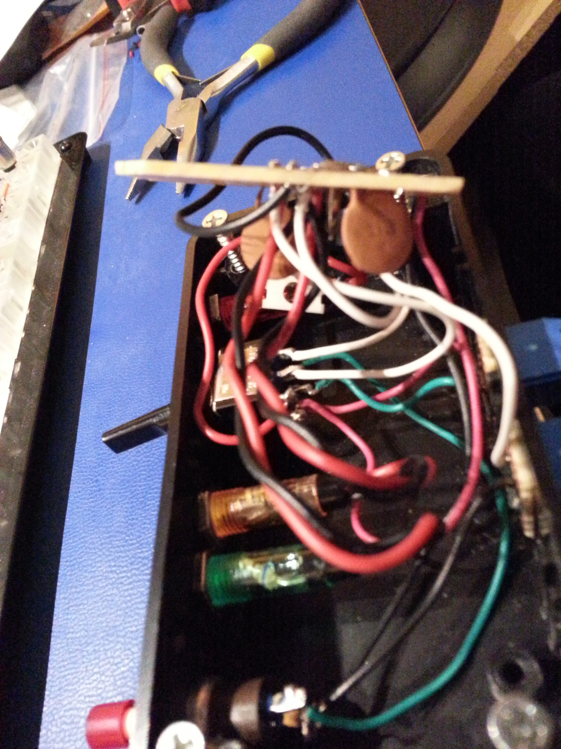
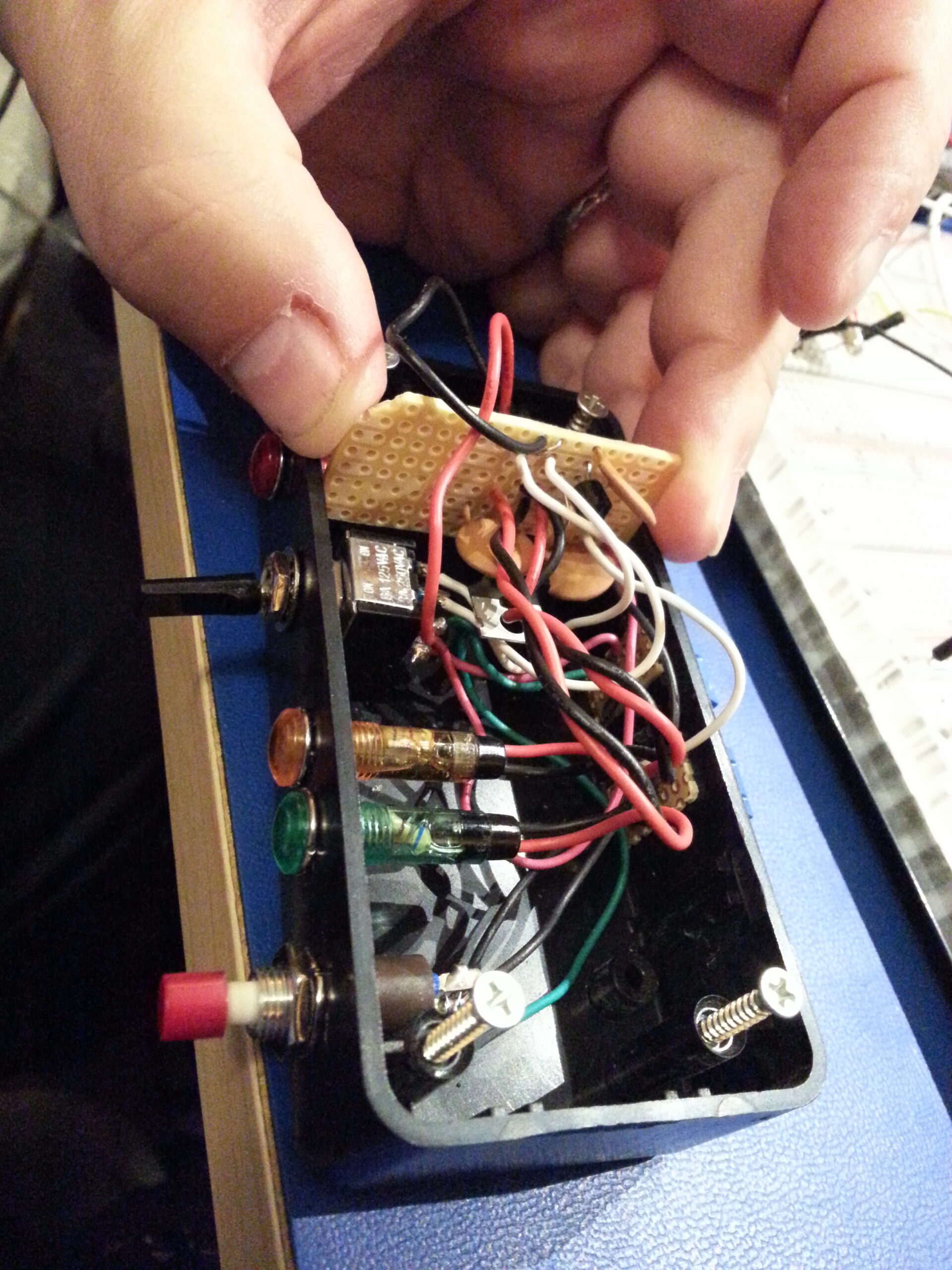
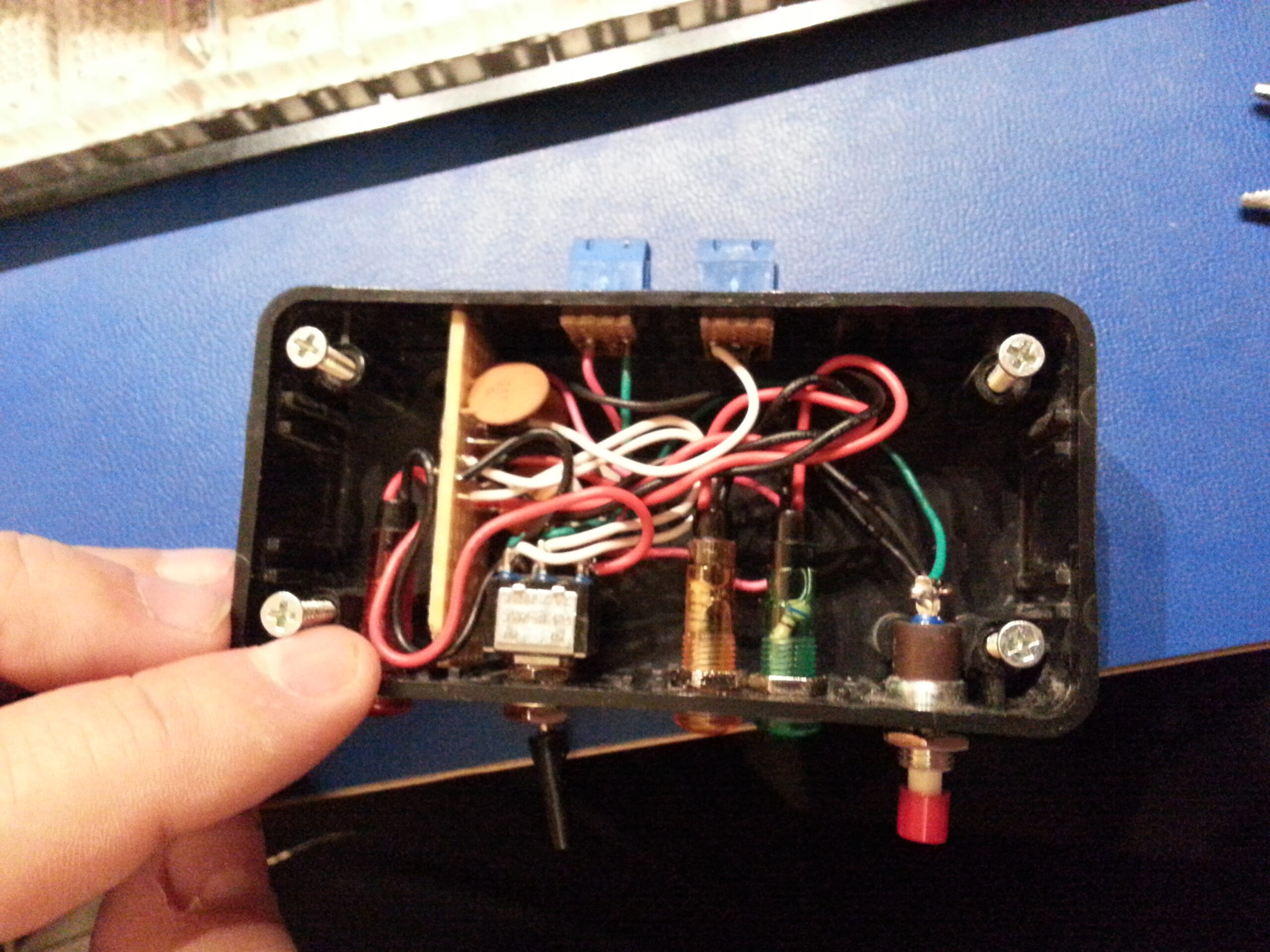
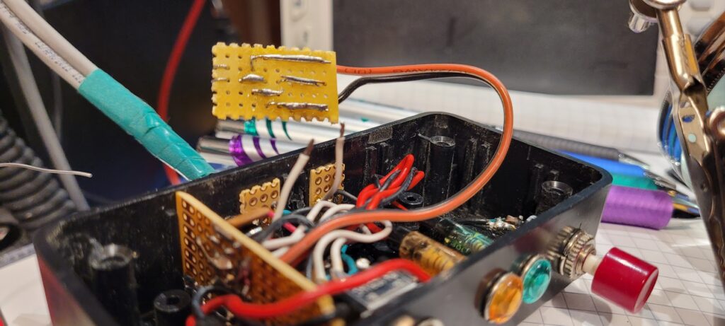
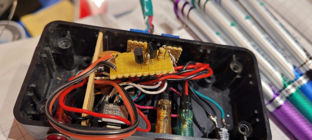
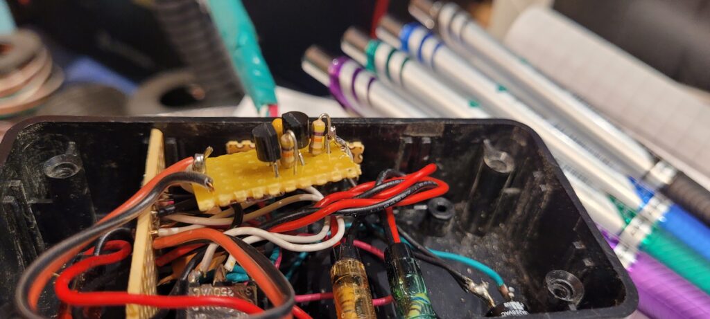
Installed
With all of the wires connected it’s time to flip the board over into it’s permanent location. Part side down, directly over the input connections. This protects the parts by keeping them (as much as possible) in free space away from the top, and makes the circuit easily accessible for any probing I might want to do later.
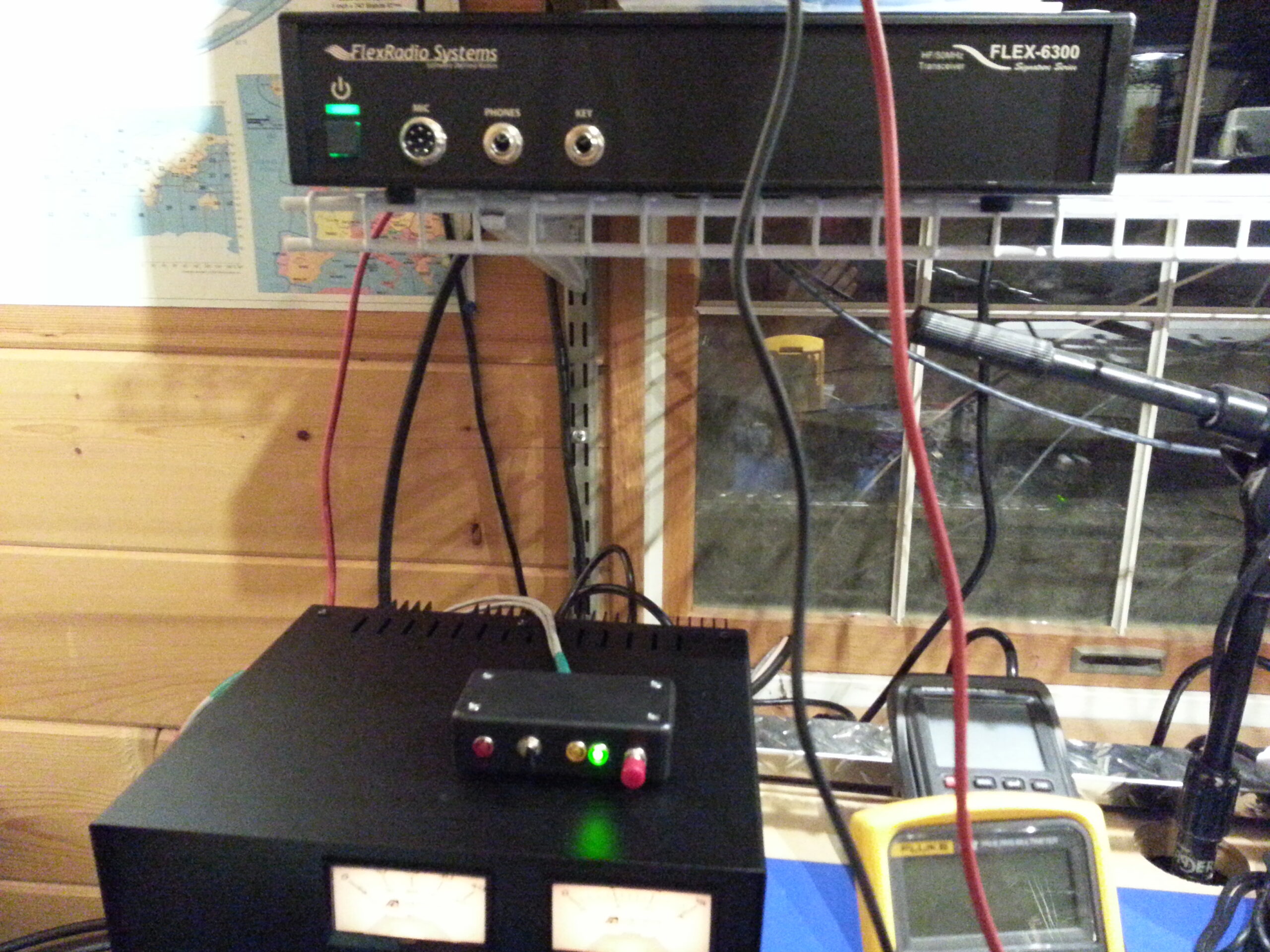
Smoke Test – Green Light!
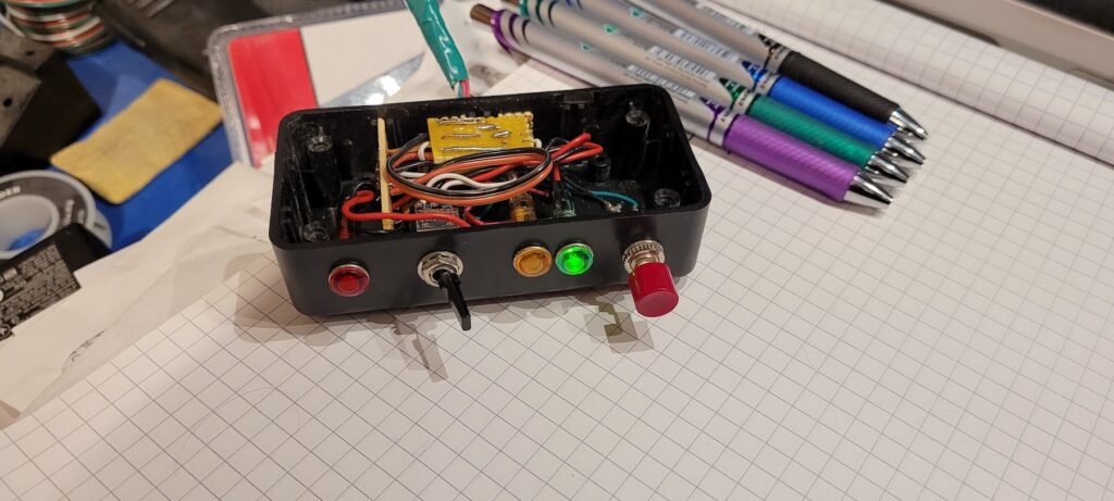
A quick look around to make sure everything still seems correct and then we turn on the power. Hurray! No magic smoke has escaped and as expected the green light is on! The tuner is virtually always in a tuned state so this is what we expect. It looks like the project is a complete success.
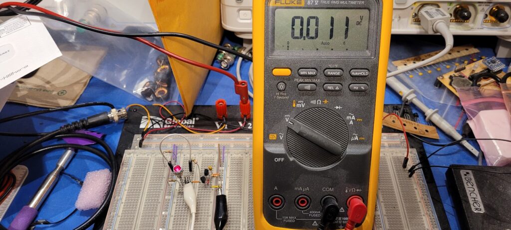
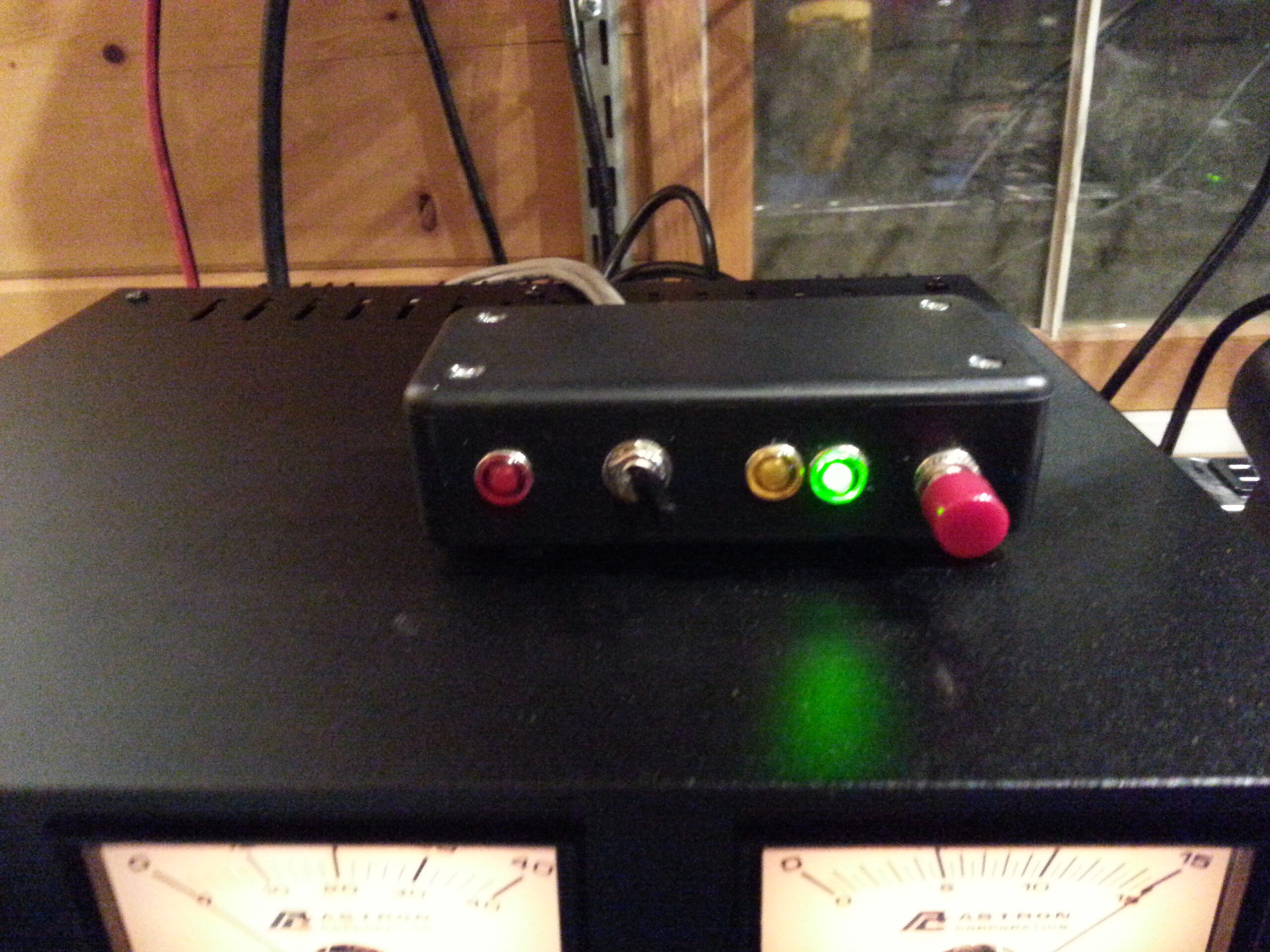
Hrmmm, That’s Not Right
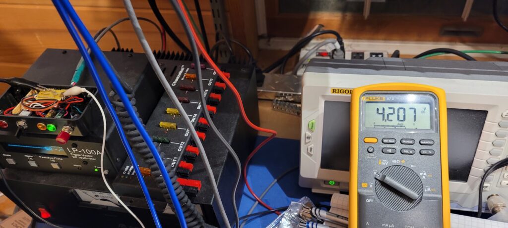
… except, after letting WSPR tune up on a few bands I notice that the green light never seems to go out. Occasionally, as I recall, the amber light should come on while the tuner is working it’s magic… and that doesn’t seem to be happening.
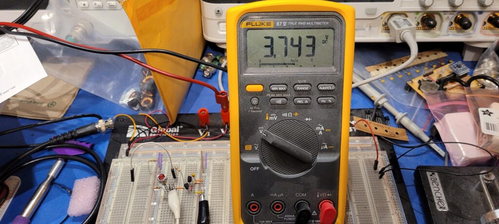
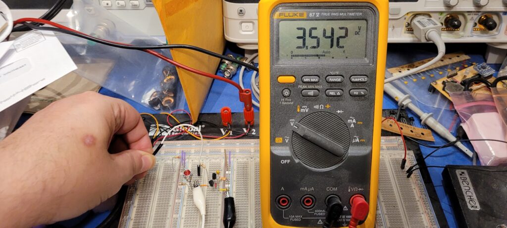
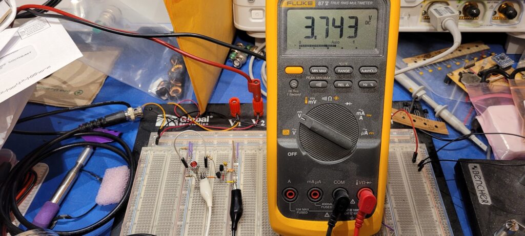
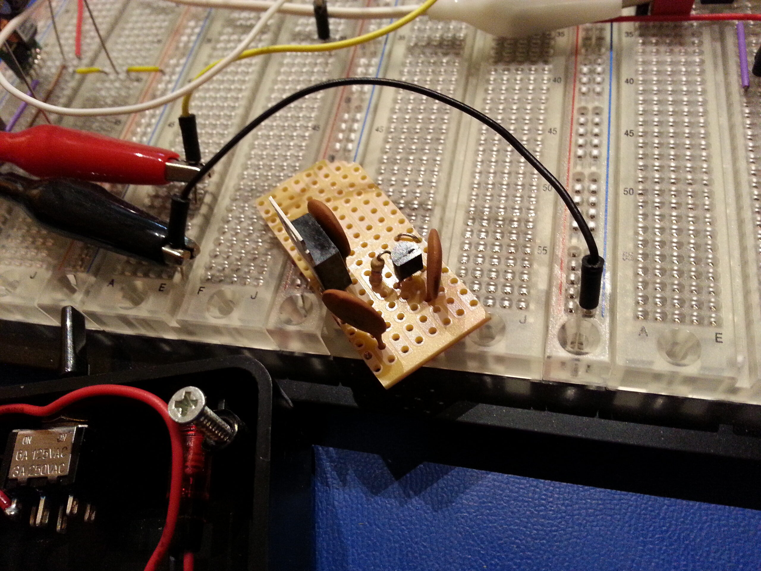
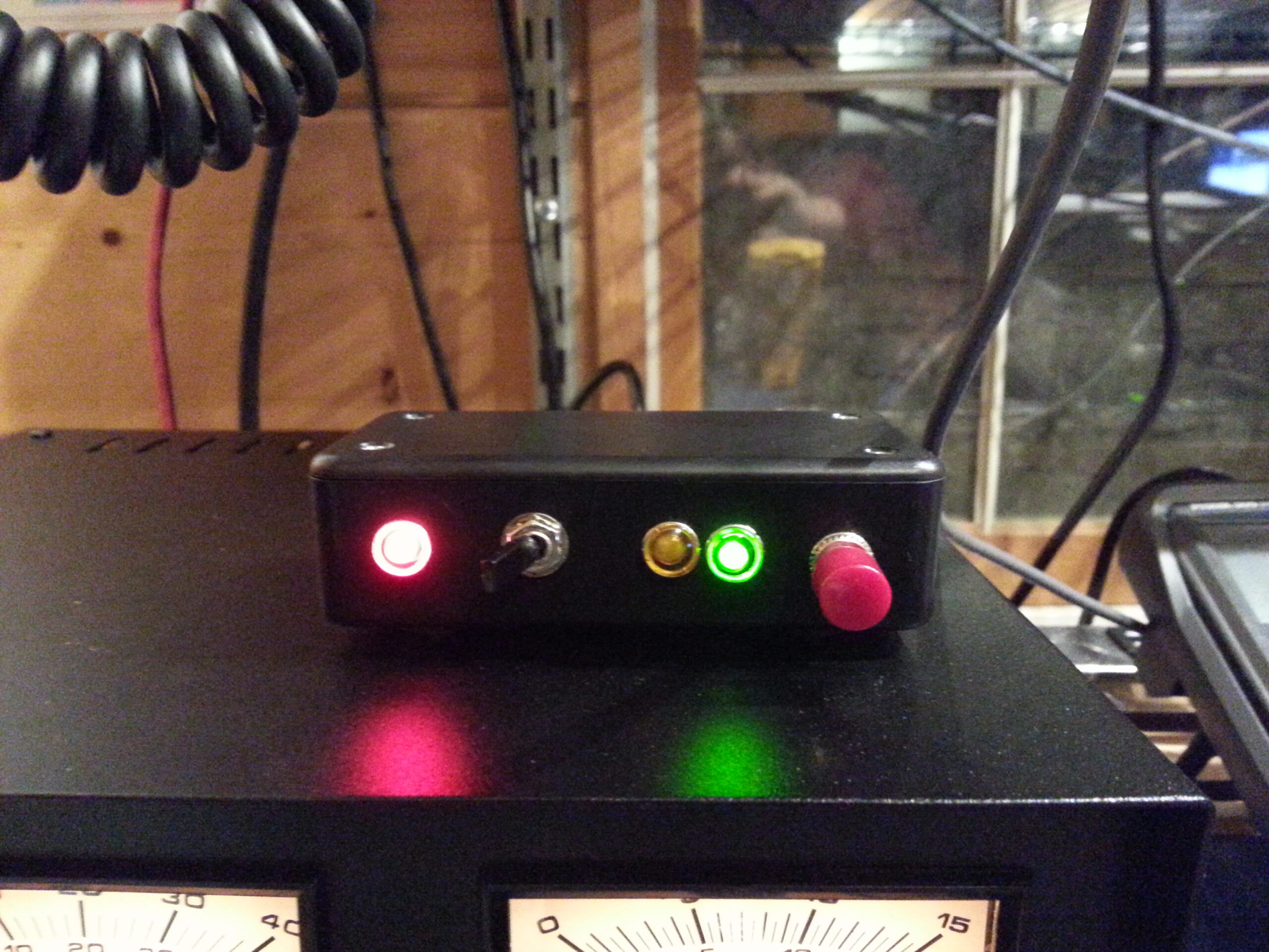
So, I hook up the meter to the input side of the amplifier via some clips and I see it’s barely a diode drop below the 5V rail… or should I say a BE (base, emitter) drop.?
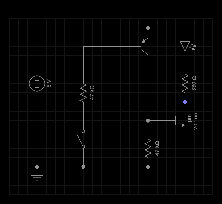
It seems that my sketchy open collector signal amplifier works too well. It’s clear that the signal line from the tuner is not open, and it’s also not shorted, nor is it being pulled to ground as expected. In previous tests I noted that the voltage did vary quite a bit as if some signal were making it through that line and into the controller… so I expected that I could amplify that signal and get the desired result.
As it turns out, that was not a good assumption… and I will have to go back to head-scratching, and perhaps go and investigate connections out near the antenna to see what’s actually happening there.
In any case, this was a fun little project and it does do what it’s designed to do… it’s just that this sketchy idea has turned out not to be the right solution. I guess that makes it a successful failure.