A while back we replaced the SGC-237 at the feed point of the big loop. Since then, the controller has been a bit sketchy. The indicator for a good tuning solution is intended to light either the yellow panel LED or the green panel LED; but since the upgrade the best it seems to manage is a bright or dim yellow.
I’m not sure what’s going on there, but I have a few theories. One is that the junction for the control indicator line in the box under the tree might be a bit oxidised causing extra resistance in the line. Another is that the design of the SGC-237 might have changed with the unit I have now, or that perhaps it never really was an open collector on the tuner end (that was a guess afterall). Another is that I just got lucky with the first design and that the long lead length might have something to do with my indicator not-quite getting the clear signal it needs.
I did measure the voltage across the input while the system was up doing it’s WSPR thing (where it must tune with each band change)… and I observed that the voltage from the indicator to ground seemed to get no higher than about 4V and no lower than about 3.2V… that’s weird, and suspiciously close to a silicon junction drop (about 0.8V)… almost as suspicious as frog’s breath… but of course, nothing is as suspicious as frog’s breath. Whatever is going on there has to do with how the indicator circuitry in my controller is interacting with the tuner through the controller cable and the junction box in the middle.
Anyway– at some point I will go out there and lie on the ground and “improve” the connections in the box. In the meantime, since the tuner seems to otherwise work just fine, I’m looking for a quick fix to get my indicator working properly again and generally make it more robust.
So, based on the idea that it’s probably some thing that looks reasonably like an open collector at the tuner end, or that even if it’s a TTL signal I might be able to interpret it like an open collector… I designed a circuit to clean up the indicator signal and make it FIRMLY on or off in an open collector manner.
Here is a snapshot of the schematic from Every Circuit (which was handier and a bit cleaner than my usual graph pad + phone camera… even if the N-Channel Mosfet symbol is a bit odd):
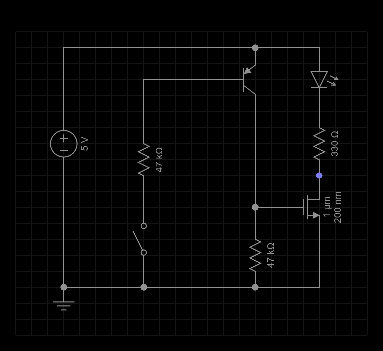
The diagram presumes I’ll be using the 5V supply from my existing controller. There is an SPST switch representing the input of the circuit which is the indicator line from the tuner. The output is the drain of the N Channel MOSFET that I’ve shown here connected to an LED via a 330 ohm resistor… but essentially that output will either be open if the input is “open” or “high”, or closed (shorted to ground) if the input is drawing current down from the 5V supply … as if it were “closed” (or trying to be) or “low” if it’s acting like a TTL signal.
Either way, the circuit should clean up the input by slamming the output fully open or closed. Here is the theory:
The input is tied to the base of a PNP transistor through a 47K resistor to limit the base current. The emitter of that transistor is tied to +5V (the positive rail).
If the input represents a high impedance between the positive rail and ground then effectively no current will flow through the base of the PNP transistor and it will be off. This will happen if either the input is something close to +5V like a TTL signal, or if the input is high impedance in general like an open collector would be.
The collector of the PNP transistor drives the gate of an N Channel MOSFET which is otherwise pulled to ground through another 47K resistor. So, if there is no current on the input then there is no current through the PNP transistor and the gate of the MOSFET will be at 0V. This will turn the MOSFET off and so it’s output will be “open” to ground.
On the other hand, if any current (even a fairly small one) flows to ground on the input, then the PNP transistor will switch on and pull up the gate on the MOSFET thus turning it on. The voltage gain of the PNP transistor given a 47K load (the MOSFET gate being essentially invisible to it) will be very high so that even a tiny current through the input will be enough to pull the MOSFET gate well above it’s “ON” voltage.
The choice of a 47K resistor on the input and also on the collector/gate is the same in both cases… it’s a high impedance (but not too high) and a handy value (I have a pretty good inventory of standard values like this). On the collector side of the PNP transistor this means a lot of gain. On the base side of the PNP transistor it means that not much current can flow through the transistor no matter what the input voltage is (within reason). That said, the beta of the PNP transistor is likely on the order of 100 so whatever the input current is at the base the output current will try to be about 100 times that amount.
I measured a 0.8v change between on and off in the existing circuit. The new circuit will amplify that by about the beta of the PNP transistor since the same resistance is on the base and on the collector, so any gain as big as 6 or so will be enough to swing the collector side between the 5V rails. With a beta of 100 I’ll be more concerned about instability than missing a weak signal. (I’ll address that if it shows up; but for now, simpler is better.)
Since I have these parts around I chose a 2N2907 (the complement of the 2N2222) as the PNP transistor; and a 2N7000 (a very common switching part) for the MOSFET.