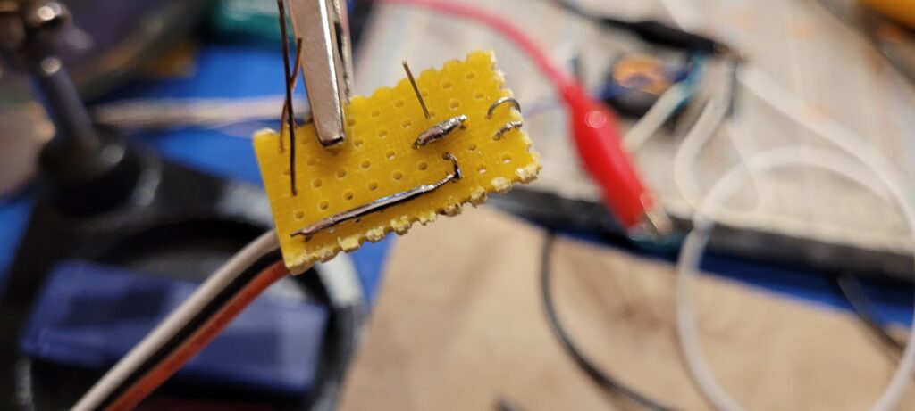
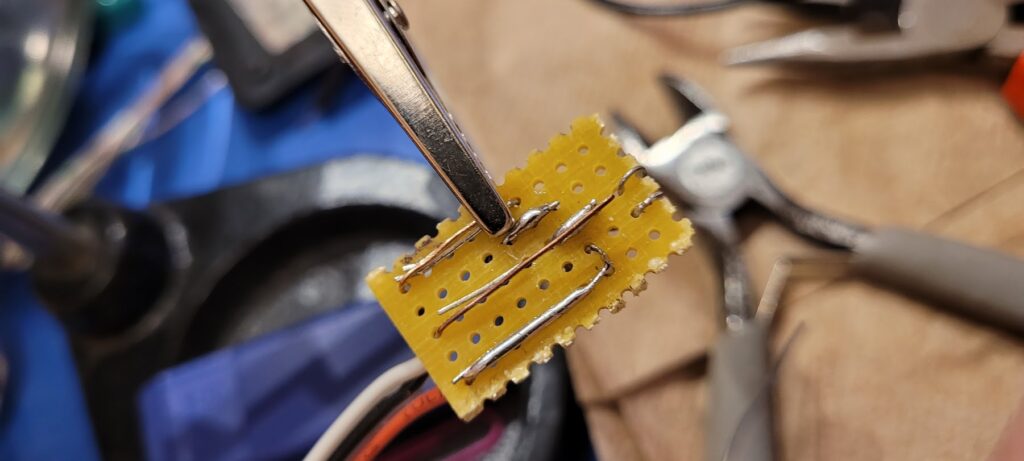
The first step to prepping for installation is to clip the sense wire used for testing and convert it into a loop – to act as a terminal on the board. The plan is to clip the existing sense wire in the controller and insert “sketchy” into that line. In order to make that work we need to have an easy way to connect both ends of the clipped sense wire. A loop on each end of the board will do nicely.
Find Power
The next step will be to identify the cleanest way to get power to our board. As it turns out the controller has regulated 5V rails in the middle of it’s board AND (lucky for us) there are two adjacent holes on those rails exactly in the right place for our ribbon wire. Here you can see the red and black ribbon wire matched up with the rails… carefully inspecting the circuit to make sure the polarity is correct and precisely where these wires will come through the controller board.
Not visible in this shot, on the top side of the board near the top of this picture I identified the 5V regulator and it’s pins to make sure which of the two rails in the middle are positive and negative.
Power Leads Inserted Top Side
Here I’ve inserted the power leads from the amplifier into the controller. They fit correctly flush up against the board and it’s clear that the colors for + (red) and – (black) match up with other connections on the board. This is another good sign that I have the polarity right.
Power Leads Inserted Bottom Side
Viewed from the bottom side we can see the wires coming through the holes in the power rails on the controller. It all looks correct (again checking carefully) so we can solder it in.
Power Leads Soldered
Here is a close up inspection of the new connections soldered into the rails. No unwanted solder bridges. Nice smooth, shiny solder joints. Some of the other nearby joints leave holes uncovered but otherwise they look fine… so I resist the urge to reheat them.
No Melted Insulation Top Side
One of the reasons I resisted the urge to re-heat those other joints is because I don’t want to begin melting insulation or causing other trouble. The connections themselves are electrically just fine – -it doesn’t matter at all (except maybe aesthetically) if the holes aren’t completely filled in. But, it DOES matter if the insulation melts potentially causing a shorting hazard.
Here we can see that the newly installed wires to power “sketchy” are not melted at all. That means there was just enough heat for just long enough to make a good solder joint.
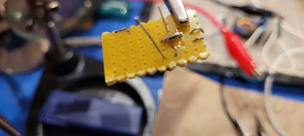
Clip Existing Sense Wire
Now that power is available to the amplifier board we need to put it in line with the sense wire. The existing sense wire is the white wire in the maw of the clippers. I have dry-fit the board into that location in the box and so I know I can clip the sense lead right in the middle of that location. One side of it will bend back to the input of the amplifier and the other side will bend back to the output. This will leave just enough extra lead to safely solder the connections and move the new board around to the right position in the box.
Carefully Calibrate Stripper
A tricky part of the installation will be trimming the insulation off of the freshly clipped sense wire. It’s important to get this right the first time… because if this step goes wrong then there will be a lot more work to do replacing that wire and it’s other connections.
The wire strippers have a small bolt and nut that can be slid into the correct position to calibrate the strippers and then tightened down. So, with the calibration bolt loosened, I take a similar wire that I can use as a gauge and carefully close the strippers on it until they just barely cut all of the insulation without nicking the conductor. Then I carefully tighten the bolt and re-check that the calibration didn’t move during that process. It seems like a lot of work – but sometimes there is no substitute and I “really” don’t want to have to replace those wires if I can avoid it so it’s worth the effort.
To make sure I have it right, I strip a few more bits of insulation off of the test wire and inspect the conductor to ensure it’s not nicked; all the while making note of the pressure required to squeeze and pull the insulation so I know what will feel right when I do the real thing.
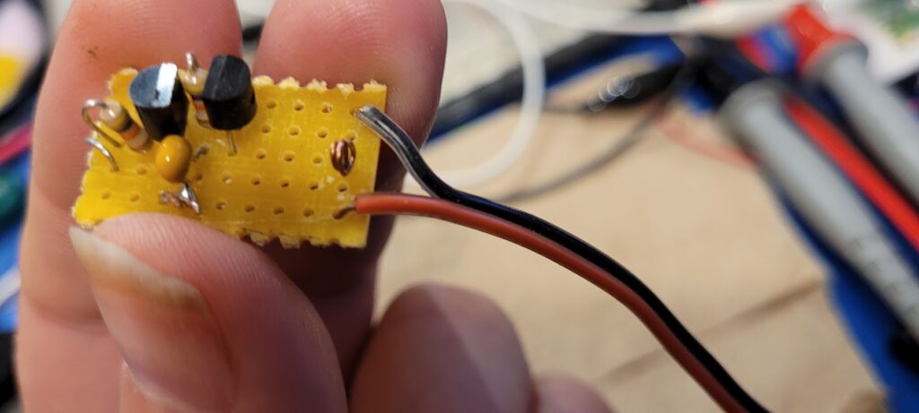
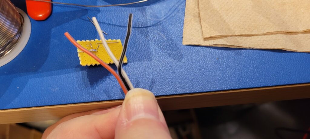
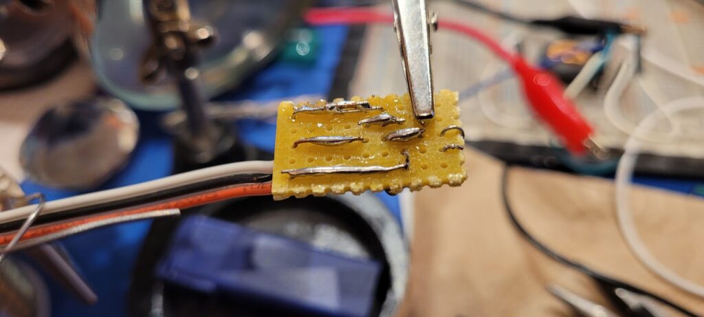
Sense Lead Cut, Stripped, and Tinned
Once I’ve stripped off about half a centimeter of insulation from both halves of the sense wire I tin the ends so that it will be easy to get these soldered into place. With tinned wires, one can push them through the connector loops and give them a quick hit with the soldering iron to get them connected. Then when both are done it’s easy to go back and re-heat them and fill them in a bit without having to worry much about the board or connections moving around during the process.
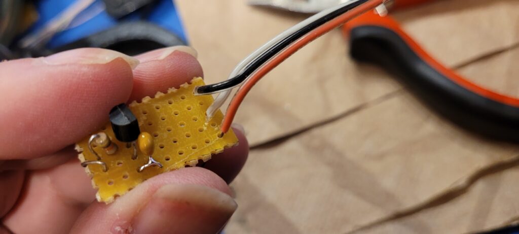
Sense Leads Inserted Into Loops
Here is a shot of the board in place, top-side up, with both ends of the sense wires “tacked” in place.
Sense Leads Soldered
With that done, we can go back and re-heat the connections and fill them in a bit to make things good and solid. Here is a shot of that from the top at about the angle I saw soldering them.
Side View
Here is a shot more from the side.
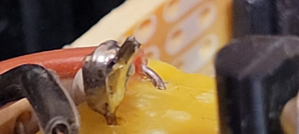
Sense Lead Output Close Insepection
Just to make sure the connections are solid I used the camera to take close-up inspection shots — here is the output lead close up.
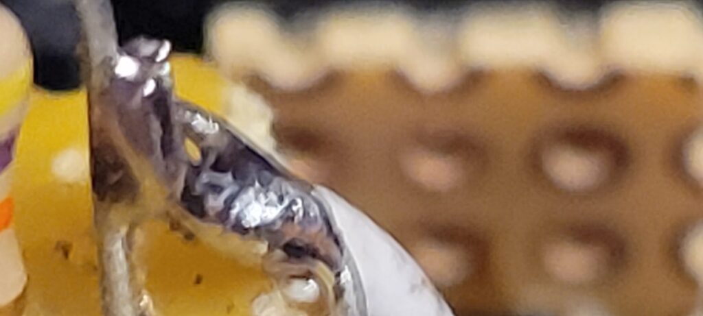
Sense Lead Input Close Inspection
Here is the input lead close up. This shot is a bit motion-blurred, but it’s clear that the connection is solid and shiny.
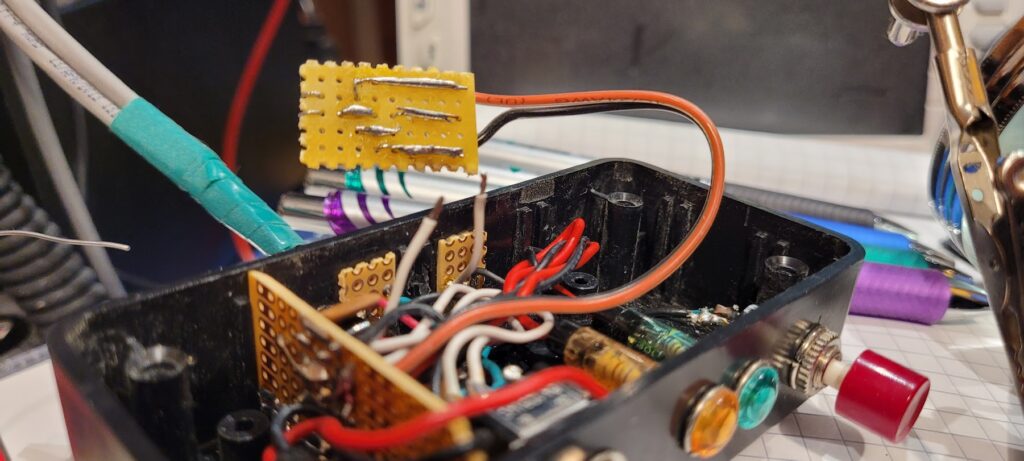
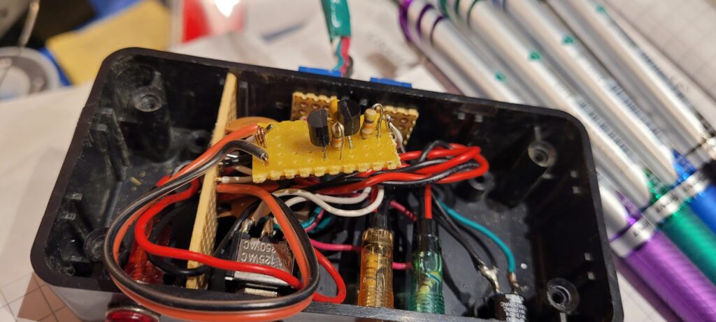
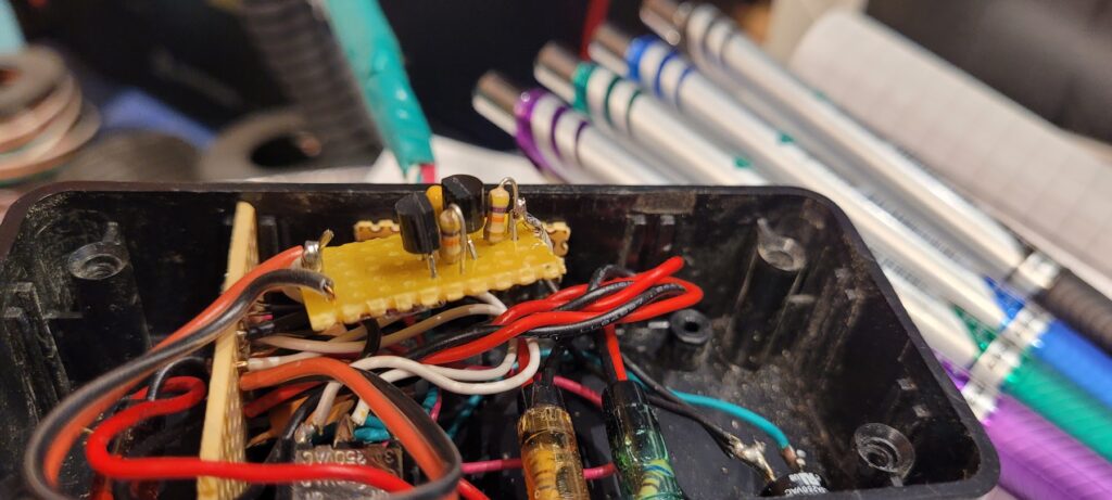
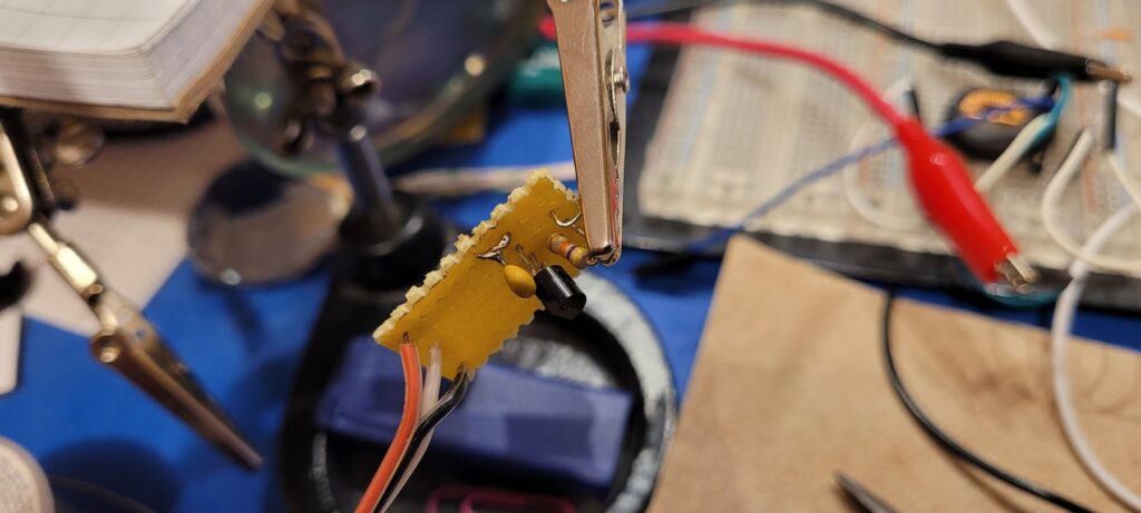
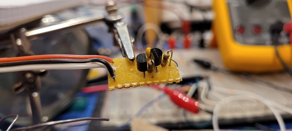
Installed
With all of the wires connected it’s time to flip the board over into it’s permanent location. Part side down, directly over the input connections. This protects the parts by keeping them (as much as possible) in free space away from the top, and makes the circuit easily accessible for any probing I might want to do later.
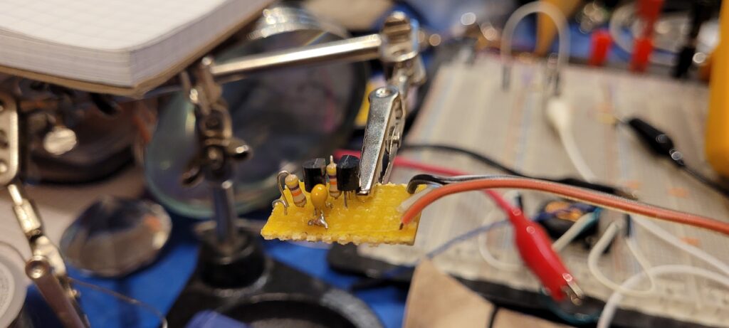
Smoke Test – Green Light!
A quick look around to make sure everything still seems correct and then we turn on the power. Hurray! No magic smoke has escaped and as expected the green light is on! The tuner is virtually always in a tuned state so this is what we expect. It looks like the project is a complete success.
Hrmmm, That’s Not Right
… except, after letting WSPR tune up on a few bands I notice that the green light never seems to go out. Occasionally, as I recall, the amber light should come on while the tuner is working it’s magic… and that doesn’t seem to be happening.
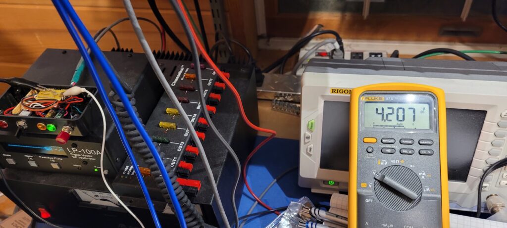
So, I hook up the meter to the input side of the amplifier via some clips and I see it’s barely a diode drop below the 5V rail… or should I say a BE (base, emitter) drop.?
It seems that my sketchy open collector signal amplifier works too well. It’s clear that the signal line from the tuner is not open, and it’s also not shorted, nor is it being pulled to ground as expected. In previous tests I noted that the voltage did vary quite a bit as if some signal were making it through that line and into the controller… so I expected that I could amplify that signal and get the desired result.
As it turns out, that was not a good assumption… and I will have to go back to head-scratching, and perhaps go and investigate connections out near the antenna to see what’s actually happening there.
In any case, this was a fun little project and it does do what it’s designed to do… it’s just that this sketchy idea has turned out not to be the right solution. I guess that makes it a successful failure.
There are a lot of ways to build quick prototypes. These days it’s even arguable that you should have a PCB made since you can get them so cheaply and quickly… and then also, if you go on to make a production grade project you’re further along.
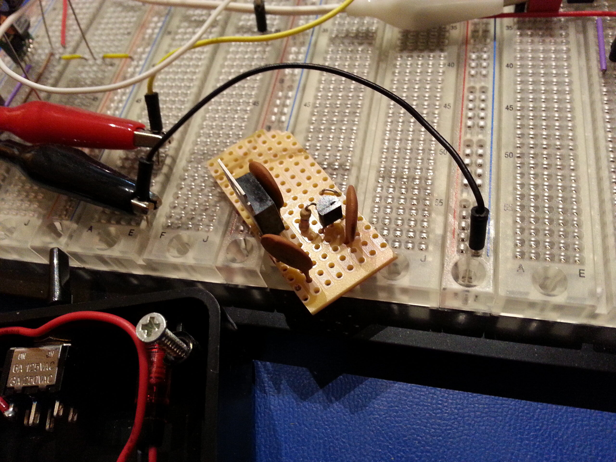
However, I decided to do something really old school and just put the parts into a perf board. This is actually a pretty rare way of doing things these days since I won’t be using any kind of purpose built prototyping PCB, nor manhattan style construction, nor any of the other popular methods. I’m not even going to use perf board pins (that’s another old-school method… can you even buy those anymore??)
Instead, I’ll plan it out so that only the component leads and a bit of wire are required. With a bit of practice this method is perfectly fine for anything that’s not going to be using RF (because there is no ground plane of any kind with this method). This method is just shy of being sculpture… but working this way is quick because it doesn’t require anything more than what you have on hand, and therapeutic because getting it all together is a bit of an art form: working with your hands, bending wires just right, growing the circuit somewhat organically one part at a time… limited only by the parts themselves, your patience, and your imagination.
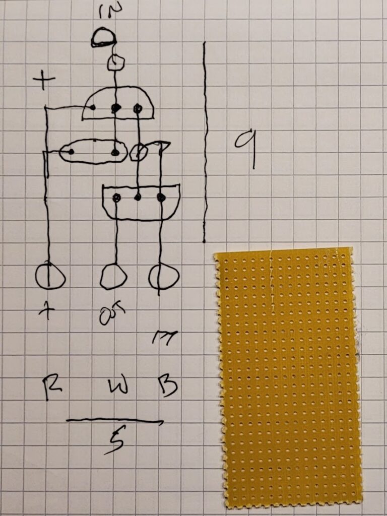
Plan the layout.
Lay a piece of perf board on a piece of graph paper, and imagine that each crossing point is a hole in the perf board. I like to work from the top side with an “x-ray” view of the wiring. Actually, the wiring might be on either side so “x-ray” means you can see it no matter where it is.
This approach will limit you to making circuits that don’t require jumpers (mostly)… and that tends to keep things simple. It’s not that you can’t use a jumper if you wish; but it’s easier if you avoid them… and that will make you think a little more carefully as you proceed.
You’ll also want to be very careful about the pin-outs of any components you’re using. Check everything more than twice as you lay out the circuit. It sometimes helps to actually pick up the part, find the correct pins, and put it in the perf board somewhere just so you can see and feel how that goes together. Not everyone can do all of that in their head (I can, but I have had a lot of practice). Seeing your drawing right next to an actual part in a board can be a very powerful way of making it all “real” so that you can reason about it without too much effort. The more time you spend relating the two physically the easier it will be (eventually) for you to see that process in your mind’s eye.
Generally proceed from input to output; complete the nets for any given component before moving on to the next (but have in mind where the next connected parts will fit into the layout); and try to keep the rails on the outside edges of the board. By working this way, eventually you will complete all of the work for one section of your design before moving on to the next section. As you complete each section it’s a good time to check that it’s really complete and everything is properly connected before moving on to the next.
Don’t be afraid to start over if you run into a dead-end of some kind… like painting yourself into a corner in a room, it’s possible to go through this process and eventually find out that you don’t have room for something; or maybe you might discover a better layout along the way. At this point it’s only paper! Toss it out and start again… this time starting from experience… it will go faster and be better each time you iterate through this process (if you need to).
After having done this for a while, I can usually get through a complete design in a single pass with almost no re-work… mostly because at this point I can see forward several steps at each stage and because I can have a rough block-diagram kind of model in mind even before I begin. All of that comes with experience and it’s the kind of thing that can save you huge amounts of time and trouble if and when you do start designing PCBs… starting with a “rats nest” and dragging parts into place, of course (you don’t use auto-routing do you!!!).
In this case, I started with the input (one resistor, yeah, not much of a section), then since it’s next connection is to the input amplifier I completed that next: first by placing the input transistor so that it’s base is right next to it’s side of the input resistor, then by adding the filter capacitor from that net to the emitter side of the transistor and the positive rail, then I cheated just a little by adding in the pull down resistor that’s at the gate of the output stage… I say I cheated but I didn’t really, it was a natural progression to the next stage and (depending on how you look at it) the collector resistor of the input amplifier IS the pull-down resistor for the gate of the output switch… either way, that part completes the input section and makes for a good time to look it over and check that all of the circuit up to that point is complete and will work as expected. A pause, then on to adding in the FET, and so forth…
I like to imagine actually mounting the parts as I draw them on the page so that when it comes time for physically mounting the parts and soldering them together I’ve already had a dry-run through that process.
This includes considering how the parts will hold each other in place through that process and when the project is completed. Some combination of bent wires against the circuit board, little loops, and other mechanical tricks will be combined to make this process work. Working out those details while laying out the design drawing is a powerful way to avoid problems during assembly and after things are complete.
By the time you’ve finished the drawing you should have complete confidence that all of the nets have been accounted for and that the physical rendering of the circuit will not only work, but might even have some aesthetic value 😉
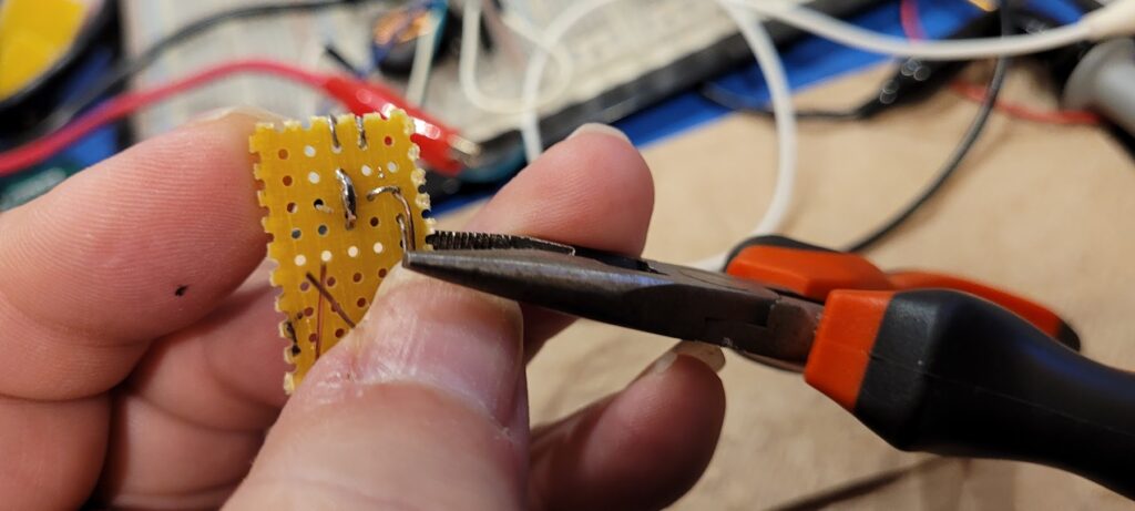
Cut out some perf board.
Once you’ve finished your drawing you will know precisely how many “holes” of your perf board are required by counting the squares on the graph paper that are taken up by the completed design. Use a marker (sharpie) to sketch out the boundaries on your perf board and then score over those with an exacto knife. After that, you should be able to fairly easily use needle nose pliers to cleanly break the perf board along those lines.
I like to use the long edge of the pliers along a scored line and start bending the board at one end of it… that usually leads to a nice clean break as the needle nose pliers will tend to protect the part of the board that they cover.
Mount the input resistor.
Right away I start with some of those little physical tricks I mentioned. One end of the input resistor must also create a terminal for connecting the input. Here, I’ve used that to physically hold the resistor in place when it’s first mounted.
Using the end-on style of mounting this resistor (as was popular in old transistor radios) I chose to put the body of the resistor close to the input transistor. This way, the other lead of the resistor makes a handy test point and also is easier to work with while weaving the end of it through the perf board and back to make an input terminal (loop). Down through one hole, up around the edge of the board and back down through an adjacent hole bent into a loop. This lead holds the input resistor into the board early and acts as a strain relief for any wire(s) that might be soldered to the terminal later.
Mount the input transistor.
Next up I added the input transistor. This being a PNP transistor, I know I want the emitter toward the positive rail (eventually), and the collector toward the negative (ground) rail. Luckily the pin out has the base in the middle so it’s really easy to get precisely what I want just by making sure the flat side is away from the input resistor and the input resistor is “in the middle.”
To hold the transistor in place I can start by slightly splaying the leads out on the underside of the board, or perhaps even bending some of them into their final direction prior to soldering.
If you look closely you’ll see another physical trick similar to what was done with the input resistor. In this case, the emitter lead is weaved through the perf board to stick up through the top side eventually to connect to the positive rail and the filter capacitor. This required a little thinking ahead and was only one of several options; but I decided it was a good way to hold the transistor in place and provide options for binding the positive rail later.
Input connections underside.
Looking at the underside you can see that the input resistor lead is bent flat against the perf board and runs right next to the base lead of the input transistor. This way, the base lead can be laid flat right next to it in the other direction making for a tidy connection and a strong physical mount for both.
You can also see off to the right of that where the emitter lead has been fed back up through the perf board to connect to the positive rail and the filter capacitor (coming up next).
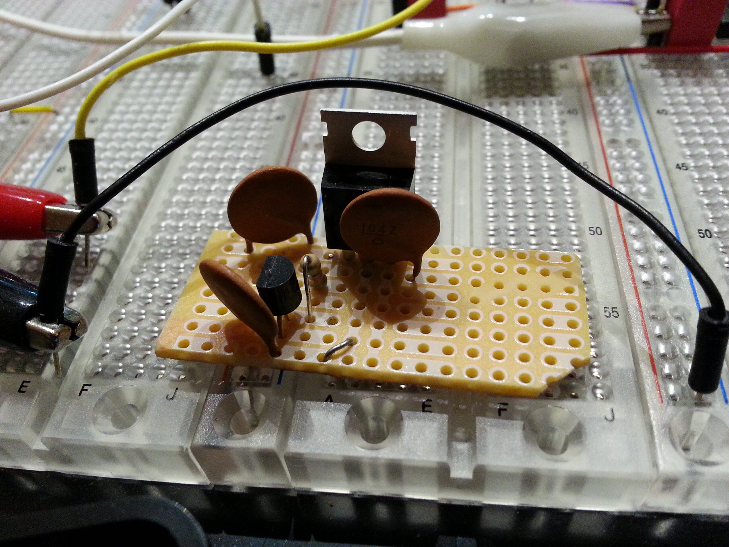
Add the filter capacitor.
Back on the topside of the board you can see how the filter capacitor fits perfectly (skipping a hole) between the extended emitter lead and the base lead. Here again was an opportunity during the planning stage to put a part through the perf board and understand exactly what size it is.
With the filter capacitor in place the emitter lead is bent down to meet it at the hole on that side. I actually tried to get the lead to go down through the same hole– but it was a bit too short and thick for that. No matter, I planned ahead so there will be plenty of ways to sure up this connection electrically.
Solder in place on the top side.
To start with, I just soldered the emitter lead to the filter cap lead on the top of the board. That works fine for these first steps and holds the filter capacitor in place while working on it’s other lead.
Connect filter capacitor to input, underside.
Back on the underside of the board the filter capacitor lead gets bent flat across the base lead and the input resistor lead. Having all three of these laying in parallel to each other will make for a good electrical connection.
Solder in place, underside.
Once soldered, the net for the base of the input amplifier is complete; and the net for the emitter side of the input amplifier is well prepped. Assembly of the circuit is progressing essentially in the same order as it’s planning was done.
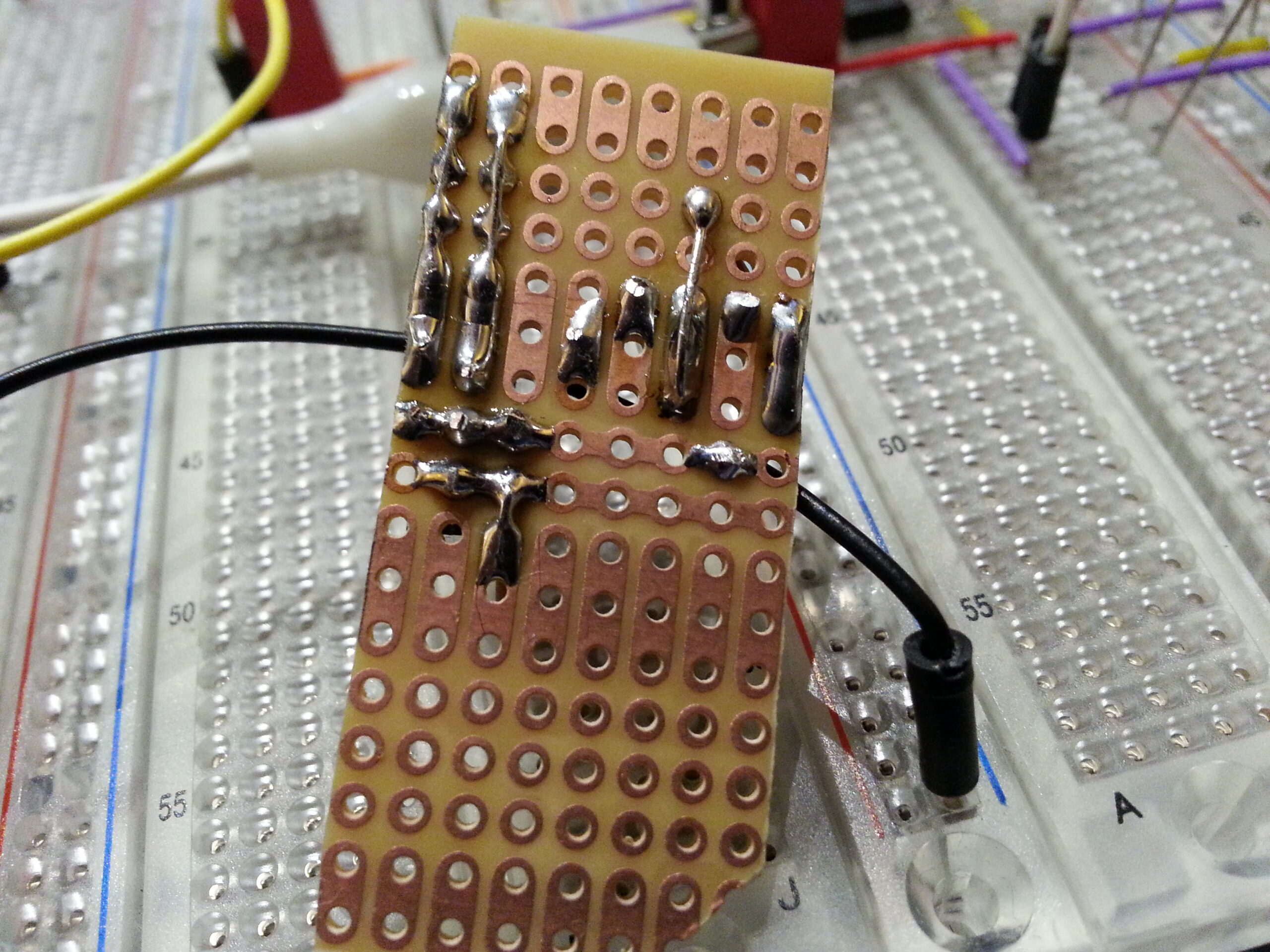
The output section is highly dependent on the power rails being in place so I decided to get that work done before installing the FET and other components. This kind-of breaks the rule of progressing from input to output… but not really since in this case best way to install the next section would be to have the power rails (the ground rail especially) in place first.
Wire for rails and output.
I happened to know I had some color coded ribbon wire when I started this so I planned to use it from the beginning. It normally has 4 conductors, but at this point I’d stripped off the green wire leaving a convenient red, black, and white. In other parts of the project the input is generally white so that works out perfectly.
The imperfect part is that the white is not in the middle– but it will be on the perf board… and as it turns out, with a little planning, even that won’t matter for long because I’ll be removing the white wire to create a terminal instead during integration. For now, however, having these all together in a ribbon will help hold things in place.
Wire for rails and output fed into board.
After stripping off sufficient insulation to reach back to the existing circuitry I put the wires through the perf board and bent their leads flat along the required straight lines on the underside.
Route the positive rail into place, underside.
The most useful next step is to complete the positive rail. Note that the wire ends up parallel to the lead from the filter capacitor; but it runs past that so that it can be fed into the hole where the emitter lead was previously woven back up through the board.
Positive rail soldered into place, underside.
Having soldered the positive rail to the filter capacitor lead, which was laid down parallel to it, and having extended that further to the emitter lead, the positive rail net is now complete and quite solid.
Reheat the emitter at the positive rail.
For good measure I reheated the emitter, filter capacitor, and positive rail on the topside of the board.
Add pull-down resistor to collector.
The next best connection to complete the input section and begin the output section is the pull-down resistor. Here you can see it mounted with it’s body at the collector of the input transistor and it’s tail going through the board in line with the negative rail.
In this case I opted to have the tail connect to ground since that is a safer thing to expose and also because it keeps the lead connected to the signal in the circuit as short as possible.
Bend pull-down resistor leads for ground rail and collector net.
Back on the underside, the tail of the pull-down resistor is extended along the path of the negative rail; and the body side lead is folded flat in parallel with the collector lead of the input transistor. The transistor lead is then extended along that path to eventually meet up with the gate of the output FET.
Solder collector lead.
With the collector lead soldered to the pull-down resistor the resistor is held solidly in place and it’s time to mount the output switch (FET).
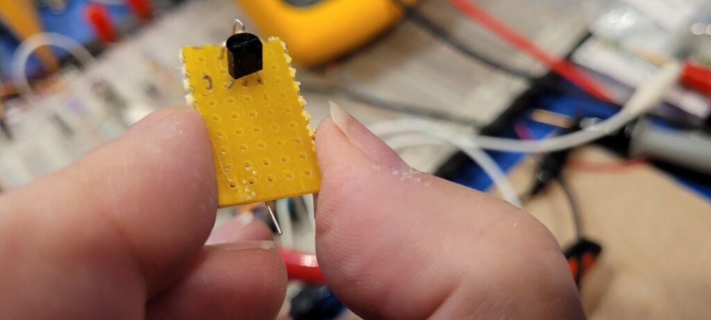
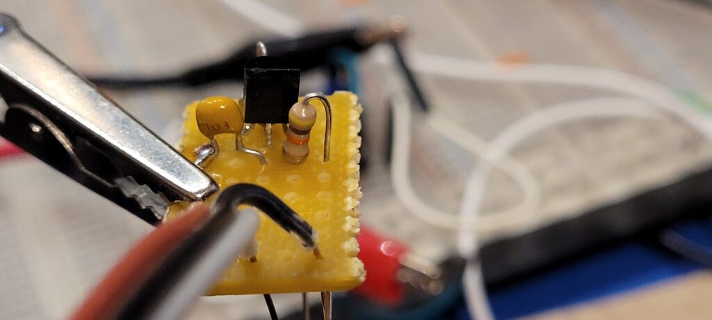
Mount FET.
The pin-out of the FET is also convenient. In this case we can put the source in line with the ground rail, put the gate in the next hole in line with the collector of the input transistor, and end up with the open drain perfectly in line with the output wire. To do this, the flat side of the FET must face the flat side of the PNP transistor… but that conveniently makes for a nice space where the pull-down resistor can live comfortably.
Bend FET leads for ground rail, collector net, and output.
Back on the underside of the board the FET leads can be bent flat against the perf board in parallel with the ground rail, the collector output of the input stage, and along the path of the output lead.
Solder the gate to finish off the collector net; prep ground rail.
At this point all of the parallel leads have been pressed and bent together. Some of them (the ground rail especially, and the output lead) are “a little squirrely” so I save them for the next step where I plan to use some clips as helping hands to get them soldered up cleanly.
Also, in keeping with the input-to-output flow of work, I soldered the gate to the collector net finally completing the input section.
Solder ground rail first pass; prep open drain output.
With a bit of patience and a strategic placement of the alligator clip I made a first pass at soldering up the ground rail. That’s enough to hold it in place and keep it tidy while working on the output line.
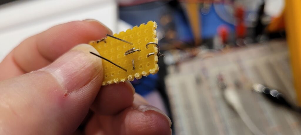
Open drain output and ground rail done.
Finally, I soldered and trimmed the output line and reheated the ground rail. That completed all of the nets! Now is a good time to inspect the work and do any final clean up that’s required.
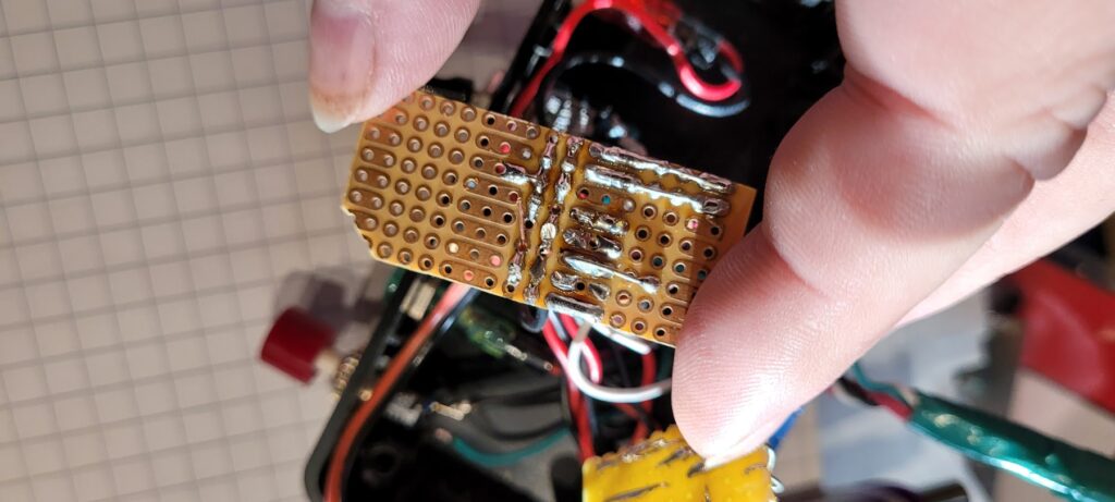
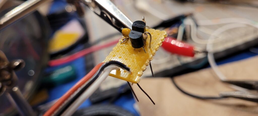
Finished view from the top, ground rail side.
Finished view from top, positive rail side.
Smoke test; input open.
Satisfied that the circuit was correct and anxious to move forward I hooked it up in place of the original prototype on the bread board, turned on the power and the meter, and made a quick test. With the input open the output is also open.
I notice that the numbers are a little different, but not by much, and I expect that having scavenged the parts for this build from those that were used in the breadboard, and that breadboards are notorious for acting differently than soldered circuits, I paid it no mind.
Open for open is GOOD! No escaping magic smoke! next test…
Smoke test; input weakly grounded.
Next I put the weak ground lead through the input terminal and I expect the circuit to close.
It works! The circuit closes, the LED comes on, and still no magic smoke!! …but did you spot the measurement error?
Just now I realize why the numbers are slightly off.
It turns out that in my excitement I put the meter in ACV mode instead of DCV. At first I was very puzzled that I got a stable reading at all… let alone one that was so close to what I expected.
I did some digging. Many (most) meters (this Fluke is one of them) don’t actually block DC when measuring ACV and so will tend to show something close to the DCV measurement when a DC input is present and an AC input is not.
Three takeaways then:
Hurray! It’s works, and it doesn’t look half bad.
Be more careful when setting up your measurements. For example, don’t ASSUME that having left your test rig set up it’s all ready to go if you just turn it on; and don’t assume that getting a measurement that’s close to what you expect is a sure sign everything is correct!
A DVM on ACV will probably (almost) measure a DCV that’s close to what you expect. Who knew?!
I thought “Ok, so let’s throw some parts at this thing and see if it works like the simulation…” and so I did:
As it turns out, I had a few different parts laying around the bench and using those would be easier than hunting down the specific values I had in my original simulation… those values aren’t critical really, so I just used what was already lying on the bench and updated the schematic in EveryCircuit to match:
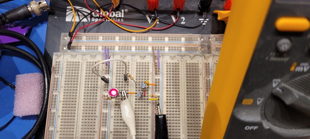
Built up on the breadboard it looked like this:
I find that with a little effort and creative thought it’s not difficult to get breadboard layouts to closely resemble schematic diagrams… and from there it’s not too much of a leap to get to what the prototype(s) and final build(s) will resemble.
A clockwise tour of the circuit on the breadboard…
Here you can see from top to bottom on the breadboard matching roughly from left to right on the schematic: There is a 47K input resistor that I’ve connected to a white wire that will act as the switch.
I describe that as a “wire” so that I can reserve the word “jumper” for the short color coded jumpers I use to make patches between segments of the breadboard. These are fantastic, by the way, because they are color coded for the number of points they span. This saves a lot of time when building up more complex circuitry or trying to trace where one or more of these jumpers go…
See the red jumper connecting 2 points away, and the orange 3, and so forth… very nice. I bought a bunch of boxes of these and I use them all the time. They’re so cheerful and perky. Full of potential – like a fresh box of colored pens and a new graph pad. I love that… but I digress.
You can see the input resistor go directly to the base of the PNP transistor, and on the back side of that transistor you can see the filter capacitor between base and emitter; an orange jumper connecting that to the positive rail 3 points away.
Moving down from there we come to the MOSFET acting as a switch. A red jumper connecting the collector of the input transistor to the gate of the switching MOSTFET and then from there you can see another 47K resistor pulling that down to the negative rail on the right.
In parallel with that a yellow jumper connects the source of the MOSFET to the negative rail (which will be common ground)… so that the other side of the switch is a typical “open drain” version of the “open collector” type of switch. The key idea being that it’s either open, or connected to ground.
Speaking of the “open drain” you can find an orange jumper crossing the centerline gap to the left and acting as the “output” of the circuit. Over on the left side you see couple of header pins stuck in the breadboard as a test point connector of sorts and then a panel mount LED connected on it’s other side to the positive rail through a 470 ohm resistor. (It was laying right there, and I didn’t care about the LED being a little bit dimmer, so I just went with it!)
You may have a little trouble spotting the header pins because there is a white alligator clip chomping on them… and if you look over to the right you’ll see a black alligator clip chomping on another set of pins plugged into the negative rail. These two clip leads make it easy to keep the DVM in circuit to measure the voltage across the output of the circuit… that way we can see just a bit more detail than whether the LED is on or off.
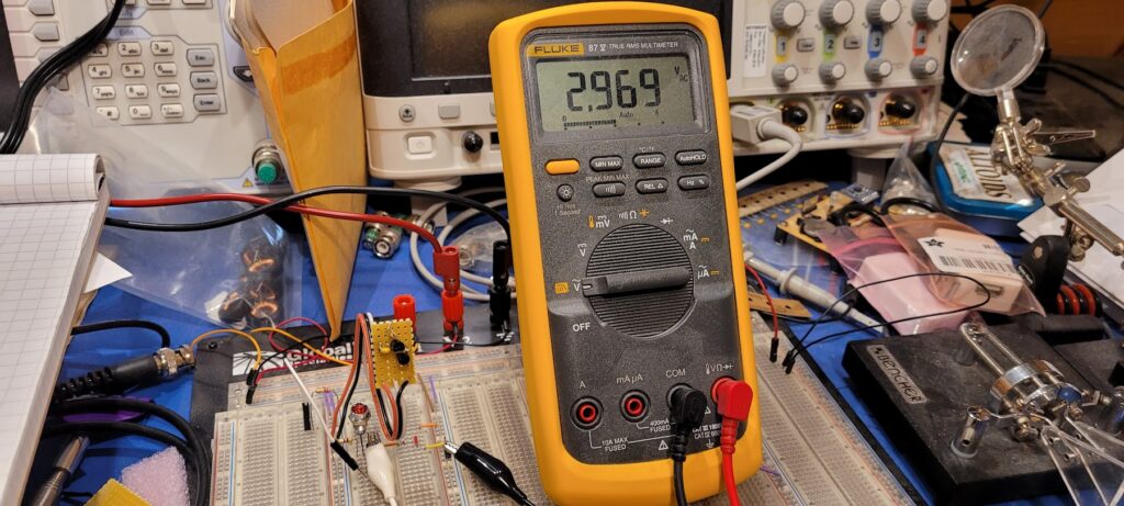
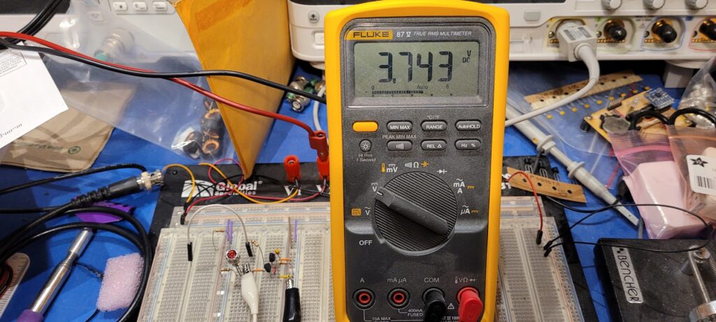
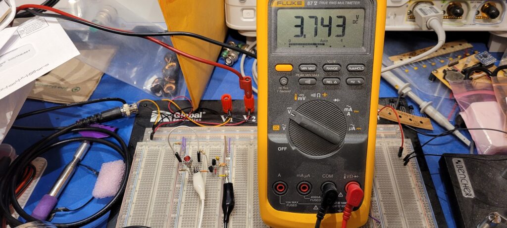
Testing Sketchy with a floating input
The guess is that the tuner controls the status line as an open-collector type of output. This means that the long wire running from the shack out to the tuner would see a very high impedance and would be essentially “floating” whenever the open collector is “off” at the tuner.
In this test you can see that the white input wire is hanging in the air on the left. The voltage at the output of our circuit is about an LED drop down from the positive rail… I guess because the DVM pulls just enough current to see that drop. 1.256v = 5 – 3.743
The LED is off… so all is well.
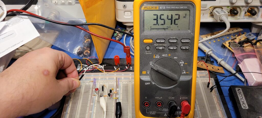
Testing Sketchy with a “human antenna” input
A long “floating” wire seems a lot like an antenna that might pick up all kinds of noise or even some stray RF (this is going to an antenna tuner after all). We want to make sure the circuit isn’t sensitive to that so we put in a filter capacitor across the BE junction of the input transistor. The idea is that the input resistor and the capacitor make a low pass filter that will reject almost anything that isn’t close to DC.
Connecting myself to the input wire to give it some “extra length” we can see that I do inject some noise; but not enough to cause the circuit to really switch. The LED stays off, and the voltage across the output only goes down by a couple hundred millivolts. That’s enough to see on a DVM, but not enough to matter when switching LEDs on and off. (Nor even enough for any logic circuit that might come later to care about it either.) 201mv = 3.743 – 3.542
Testing Sketchy with the input pulled high
Another design spec is that the circuit should be happy with a TTL input. So, connecting the input to the positive rail (+5V) we get the same result as the floating input: The output is off as expected!!
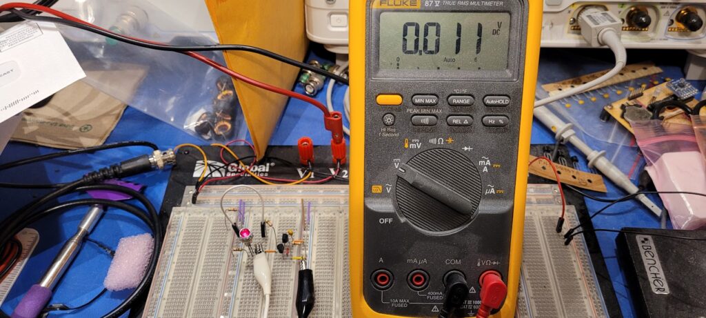
Testing Sketchy with the input pulled low
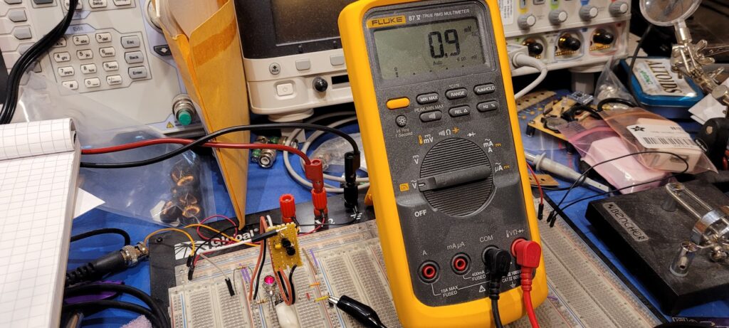
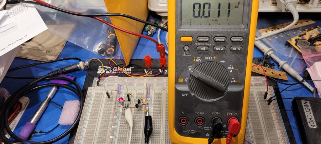
Testing the other side of the TTL input spec as well as the open collector input spec, we pull the input low by connecting it to the negative (ground / common) rail. As expected, the output goes to ground and the LED comes on!! Not only on, but VERY on… 11mv measured across the output.
This is a benefit of using a good switching MOSFET vs a bipolar transistor for this kind of output (open drain/collector). The “closed circuit” or “on” condition of the output with the MOSFET will have a much lower voltage than you can get from a bipolar transistor. Definitely closer to ground.
Testing Sketchy with the input pulled low weakly
Finally, since our theory about the status line problem is that it may be oxidized at the connector near the tuner, we tested again with a high resistance in place. In this case, a 220K resistor to simulate whatever that unwelcome resistance might be out there. Again success! The LED is fully on just as if the input had been pulled hard to ground.
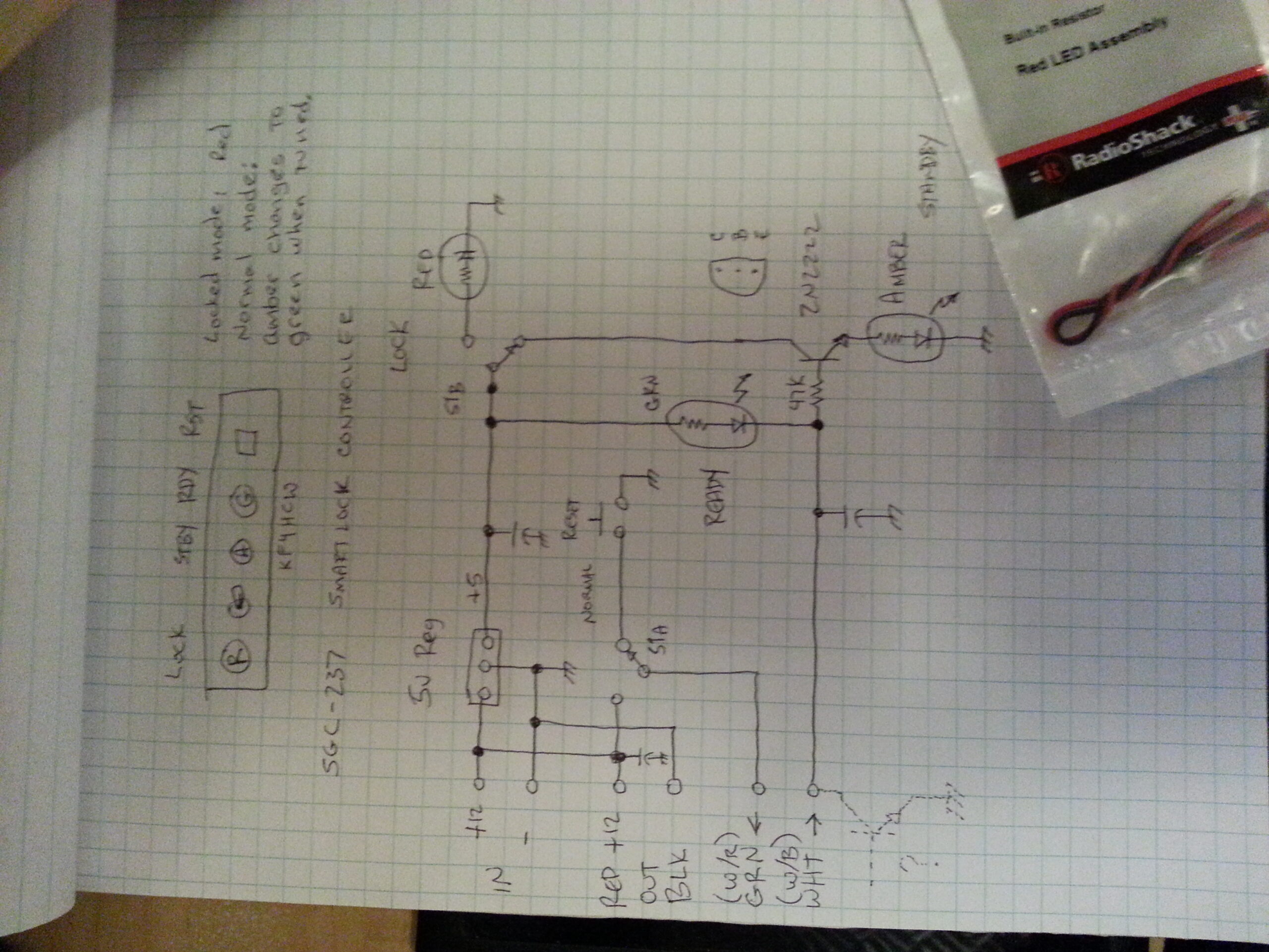
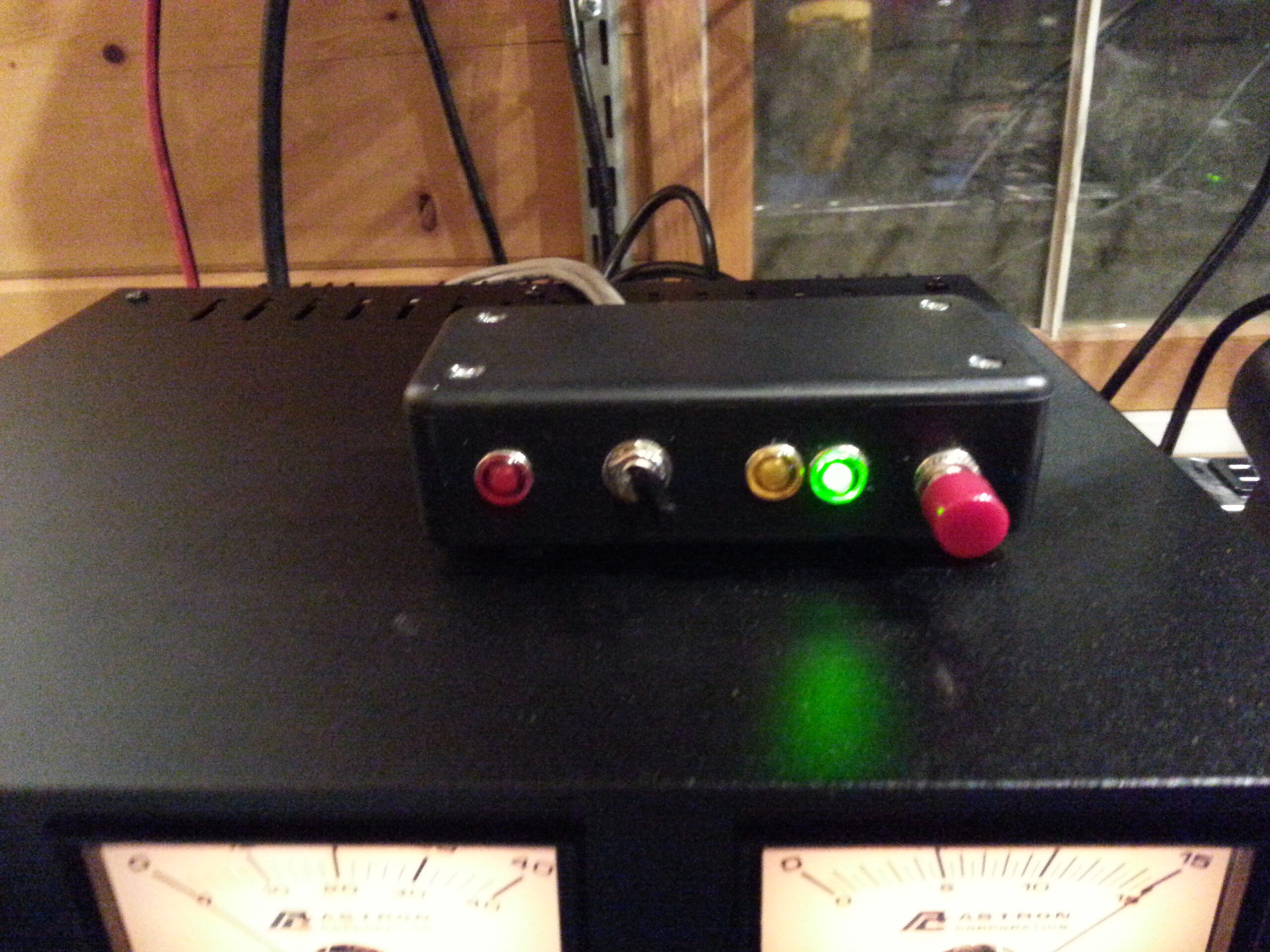
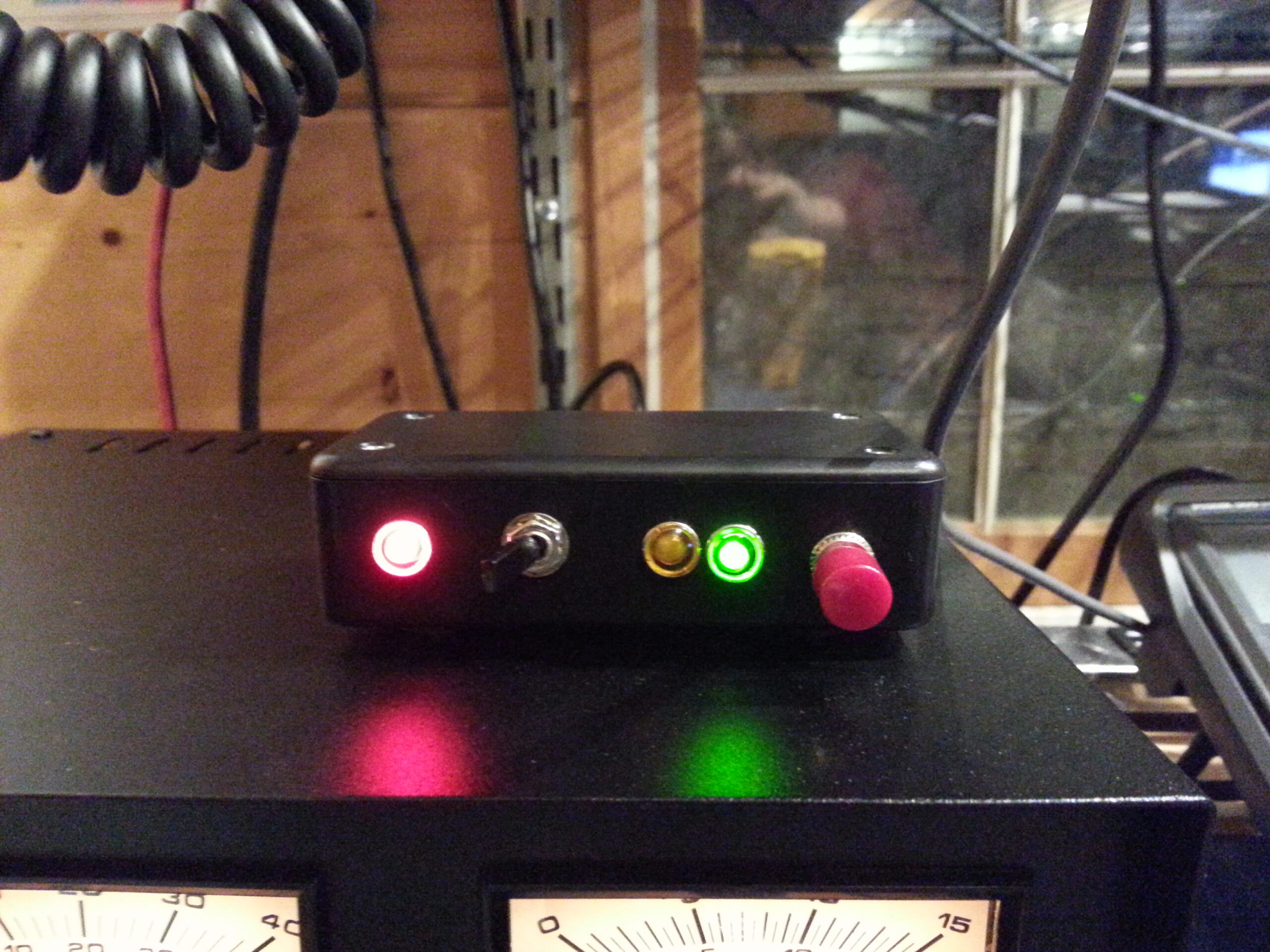
A while back we replaced the SGC-237 at the feed point of the big loop. Since then, the controller has been a bit sketchy. The indicator for a good tuning solution is intended to light either the yellow panel LED or the green panel LED; but since the upgrade the best it seems to manage is a bright or dim yellow.
I’m not sure what’s going on there, but I have a few theories. One is that the junction for the control indicator line in the box under the tree might be a bit oxidised causing extra resistance in the line. Another is that the design of the SGC-237 might have changed with the unit I have now, or that perhaps it never really was an open collector on the tuner end (that was a guess afterall). Another is that I just got lucky with the first design and that the long lead length might have something to do with my indicator not-quite getting the clear signal it needs.
I did measure the voltage across the input while the system was up doing it’s WSPR thing (where it must tune with each band change)… and I observed that the voltage from the indicator to ground seemed to get no higher than about 4V and no lower than about 3.2V… that’s weird, and suspiciously close to a silicon junction drop (about 0.8V)… almost as suspicious as frog’s breath… but of course, nothing is as suspicious as frog’s breath. Whatever is going on there has to do with how the indicator circuitry in my controller is interacting with the tuner through the controller cable and the junction box in the middle.
Anyway– at some point I will go out there and lie on the ground and “improve” the connections in the box. In the meantime, since the tuner seems to otherwise work just fine, I’m looking for a quick fix to get my indicator working properly again and generally make it more robust.
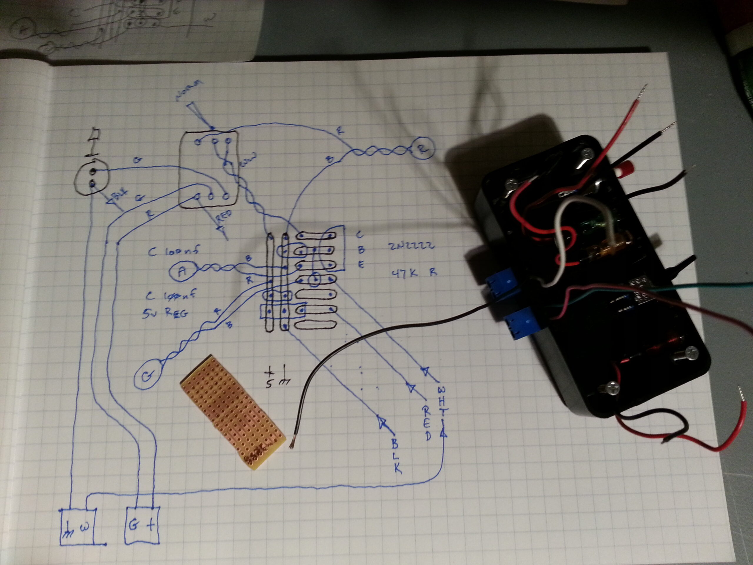
So, based on the idea that it’s probably some thing that looks reasonably like an open collector at the tuner end, or that even if it’s a TTL signal I might be able to interpret it like an open collector… I designed a circuit to clean up the indicator signal and make it FIRMLY on or off in an open collector manner.
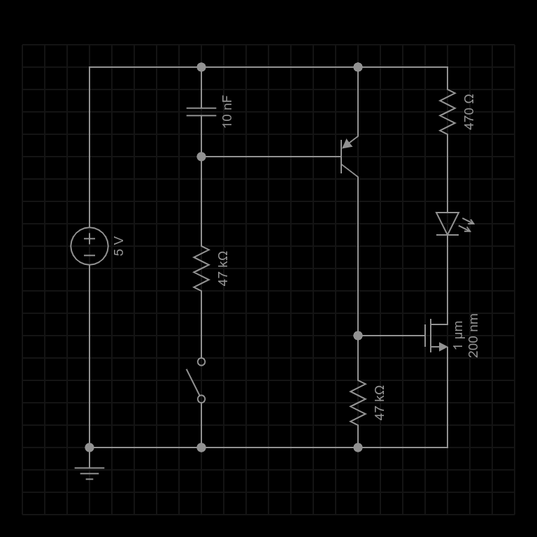
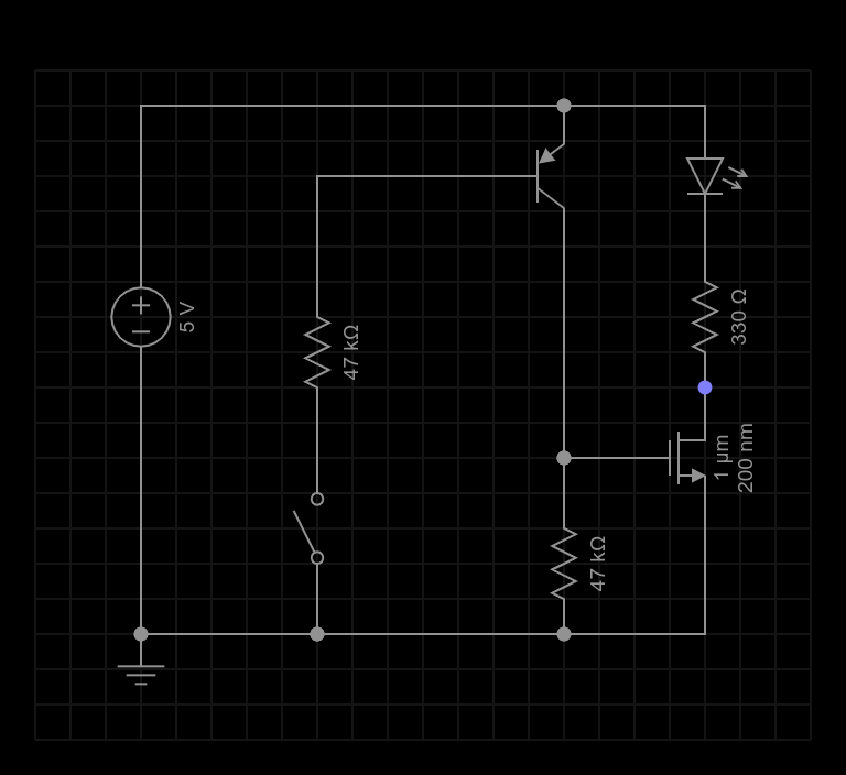
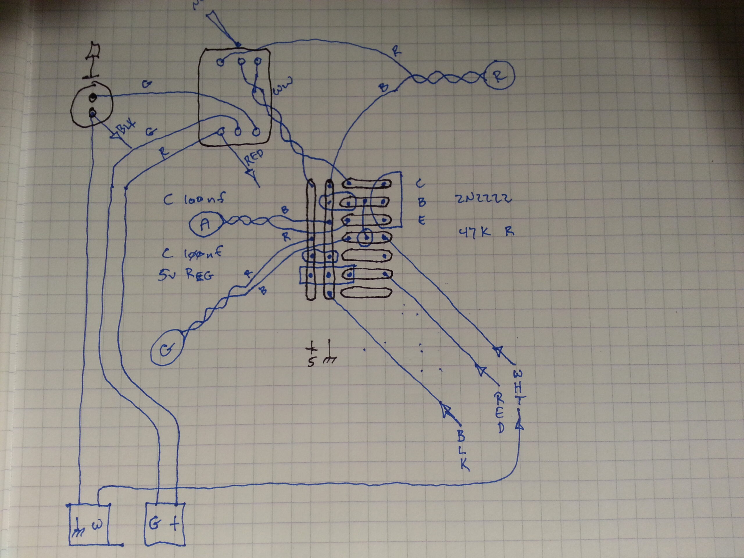
Here is a snapshot of the schematic from Every Circuit (which was handier and a bit cleaner than my usual graph pad + phone camera… even if the N-Channel Mosfet symbol is a bit odd):
The diagram presumes I’ll be using the 5V supply from my existing controller. There is an SPST switch representing the input of the circuit which is the indicator line from the tuner. The output is the drain of the N Channel MOSFET that I’ve shown here connected to an LED via a 330 ohm resistor… but essentially that output will either be open if the input is “open” or “high”, or closed (shorted to ground) if the input is drawing current down from the 5V supply … as if it were “closed” (or trying to be) or “low” if it’s acting like a TTL signal.
Either way, the circuit should clean up the input by slamming the output fully open or closed. Here is the theory:
The input is tied to the base of a PNP transistor through a 47K resistor to limit the base current. The emitter of that transistor is tied to +5V (the positive rail).
If the input represents a high impedance between the positive rail and ground then effectively no current will flow through the base of the PNP transistor and it will be off. This will happen if either the input is something close to +5V like a TTL signal, or if the input is high impedance in general like an open collector would be.
The collector of the PNP transistor drives the gate of an N Channel MOSFET which is otherwise pulled to ground through another 47K resistor. So, if there is no current on the input then there is no current through the PNP transistor and the gate of the MOSFET will be at 0V. This will turn the MOSFET off and so it’s output will be “open” to ground.
On the other hand, if any current (even a fairly small one) flows to ground on the input, then the PNP transistor will switch on and pull up the gate on the MOSFET thus turning it on. The voltage gain of the PNP transistor given a 47K load (the MOSFET gate being essentially invisible to it) will be very high so that even a tiny current through the input will be enough to pull the MOSFET gate well above it’s “ON” voltage.
The choice of a 47K resistor on the input and also on the collector/gate is the same in both cases… it’s a high impedance (but not too high) and a handy value (I have a pretty good inventory of standard values like this). On the collector side of the PNP transistor this means a lot of gain. On the base side of the PNP transistor it means that not much current can flow through the transistor no matter what the input voltage is (within reason). That said, the beta of the PNP transistor is likely on the order of 100 so whatever the input current is at the base the output current will try to be about 100 times that amount.
I measured a 0.8v change between on and off in the existing circuit. The new circuit will amplify that by about the beta of the PNP transistor since the same resistance is on the base and on the collector, so any gain as big as 6 or so will be enough to swing the collector side between the 5V rails. With a beta of 100 I’ll be more concerned about instability than missing a weak signal. (I’ll address that if it shows up; but for now, simpler is better.)
Since I have these parts around I chose a 2N2907 (the complement of the 2N2222) as the PNP transistor; and a 2N7000 (a very common switching part) for the MOSFET.
The tuner can be run without a controller, but it offers a few features with a controller that are useful (and sometimes important) in practice. I took a look at the controller suggested in the manual and re-designed it a bit to better suit my purposes. First, because I wanted to use parts that I had laying around the lab, and second because I wanted a better “light-show.”
The important features are:
You can tell the tuner when NOT to tune. I find in practice that this can be particularly important when running digital modes as switching things around at the antenna can inject unwanted noise to your transmitted signal.
The tuner can tell you when it’s found a good tuning solution. Sure, it seems like this would be obvious enough once the SWR stops bouncing around… but it is awfully handy to have a nice green light tell you when the tuner has stopped looking.
I found this out AFTER I built my controller – The tuner can tell you when it didn’t find a solution but has given up trying! On my tuner controller there is an amber light for when the tuner doesn’t yet have a solution and a green one for when it has found a solution. One day I saw these flashing back and forth like it was shaking its’ head. I figured out that’s what it does when it gives up trying. This doesn’t seem to be documented anywhere, but it’s also a nice feature.
The first step was to draw up a schematic for the circuit and do a little math to make sure everything would work.
In the controller recommended in the manual they roll their own ~9 v regulator using a zener diode and an NPN transistor. They only use this to drive their LEDs, so I did something similar but instead used an actual 5V regulator.
The next thing I changed was the “tuned” indicator logic. Their controller pulls one side of their tuned indicator to ground when the tuner is happy. I presume this is done through something like an open collector in the tuner.
I wanted two lights instead of one so I added a 2N2222 transistor and a resistor to turn on an amber “not-tuned” LED when the green “tuned” LED is not on. Basically, the green LED and its’ current limiting resistor act like a pull-up resistor to bias the transistor on whenever the “tuned” LED is not pulled to ground by the tuner. The 47K resistor in series with the base ensures that any current that flows is tiny enough that the green LED won’t light (at least not in a way you can see it). The gain of the transistor is high enough that it will still effectively saturate in this condition thus turning on the amber “not-tuned” LED.
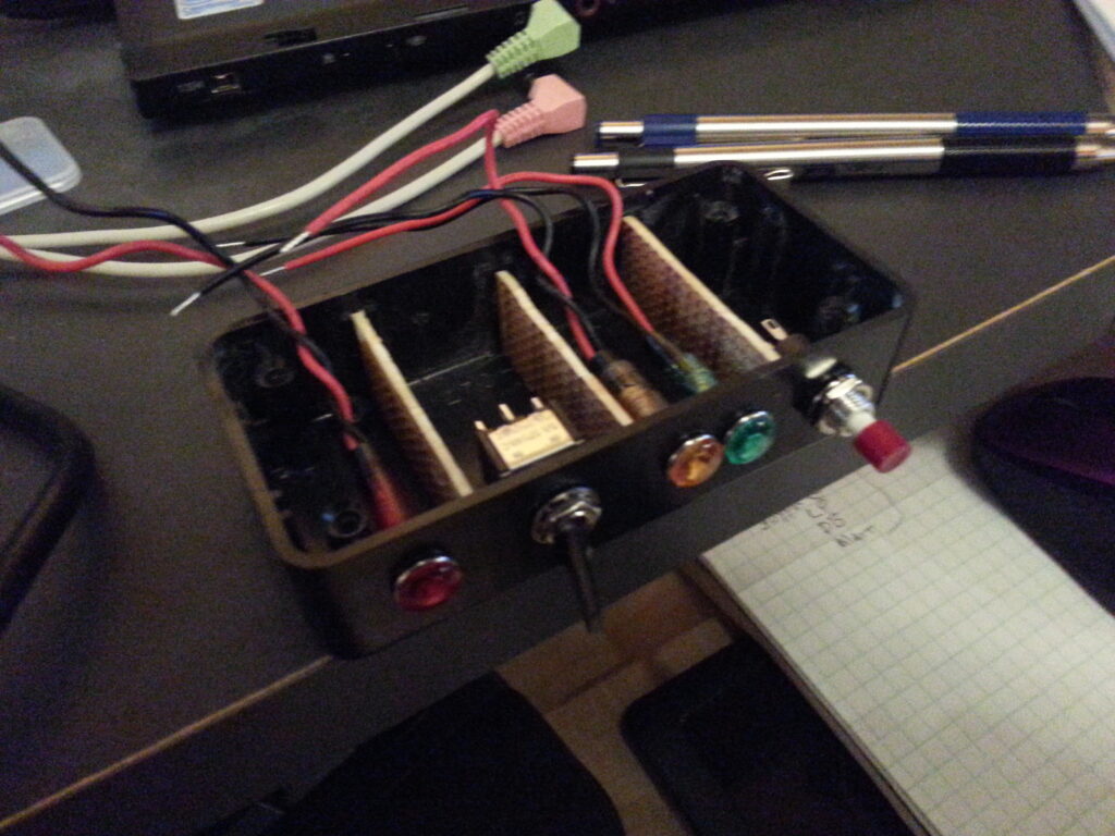
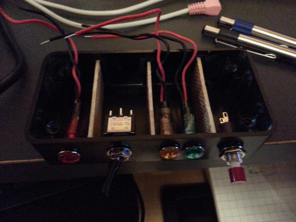
The rest of the circuit is essentially the same as their controller – so the tuner sees almost precisely the same signals. This consists of a DPDT switch, a momentary SPST push-button, and a handful of decoupling caps. All of this, a handy box, and some LEDs with built-in current limiting resistors were all handy in my lab… courtesy of the recently (at the time) defunct local Radio Shack – and my irresistible urge to grab everything I could from them in their last days.
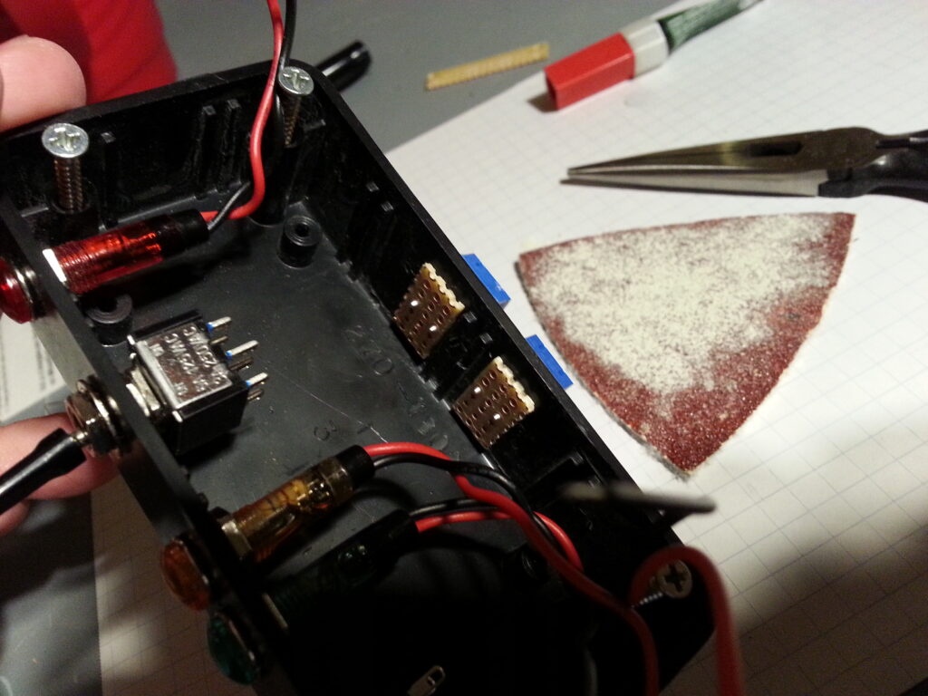
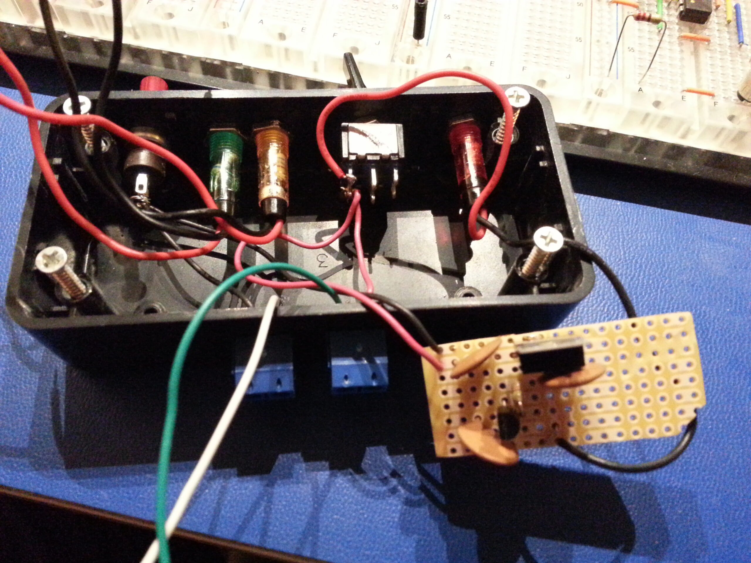
Once the design was done it was time to put the mechanical components into the box and see how they all fit. Here is where some on-the-fly creativity was required because one cannot always be sure what parts they have nor how they can be used to solve a particular problem… I mean, I wasn’t building this from a BOM where I could order up precisely what I wanted right?! I had to see what I had around and improvise with that.
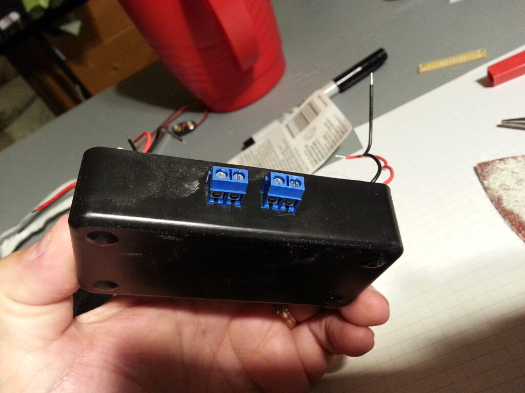
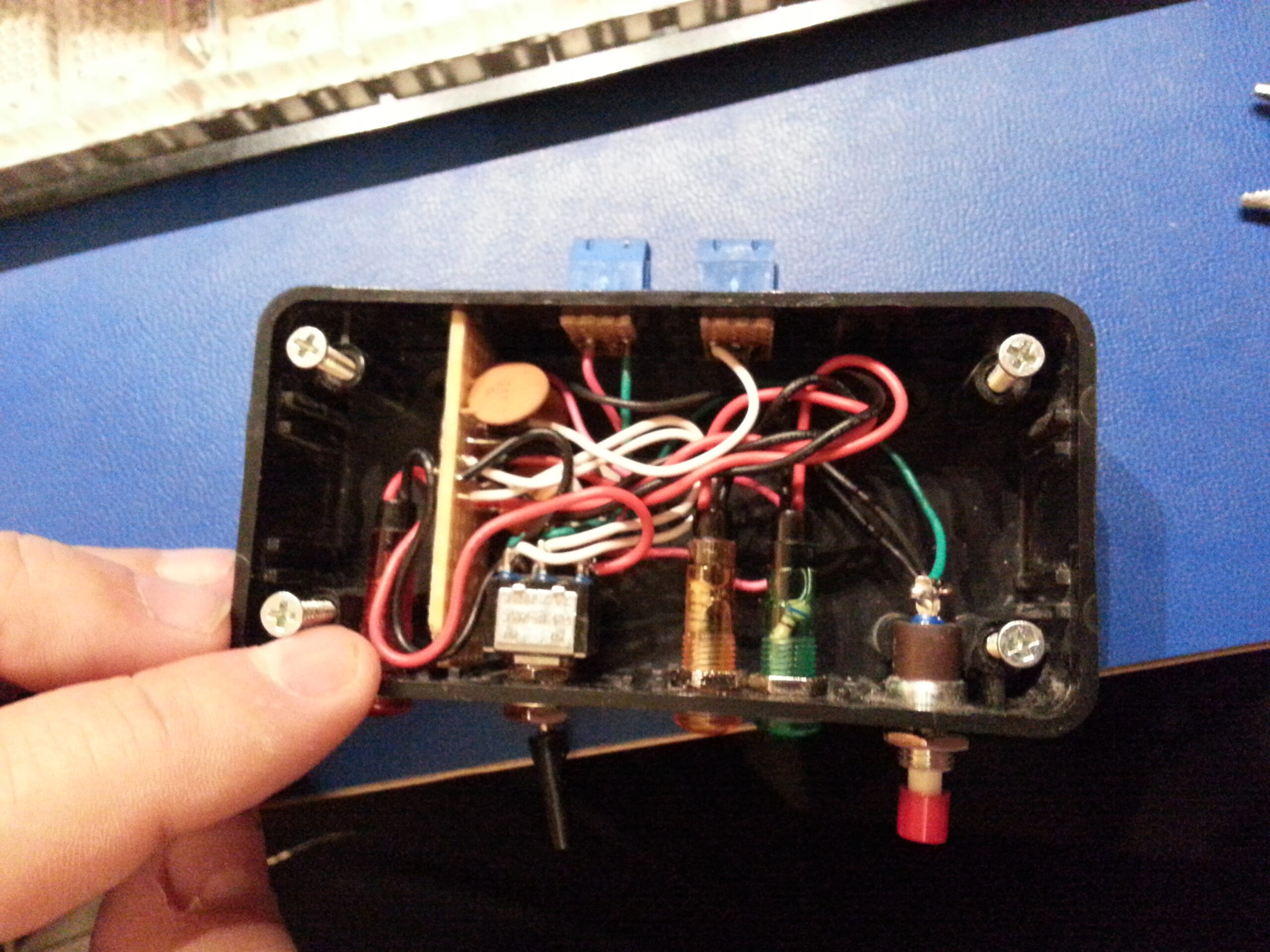
As it turns out all of the parts I had handy fit perfectly including some PCB mounted screw terminals that I was able to adapt to the back of the box with a little bit of drilling, sanding, and some small pieces of protoboard.
Next up I designed the layout of the electronics on another piece of proto-board. It’s always a good idea to take this extra step rather than going directly to soldering parts in place – even on something simple like this. The end result almost always turns out better and cleaner for the extra effort.
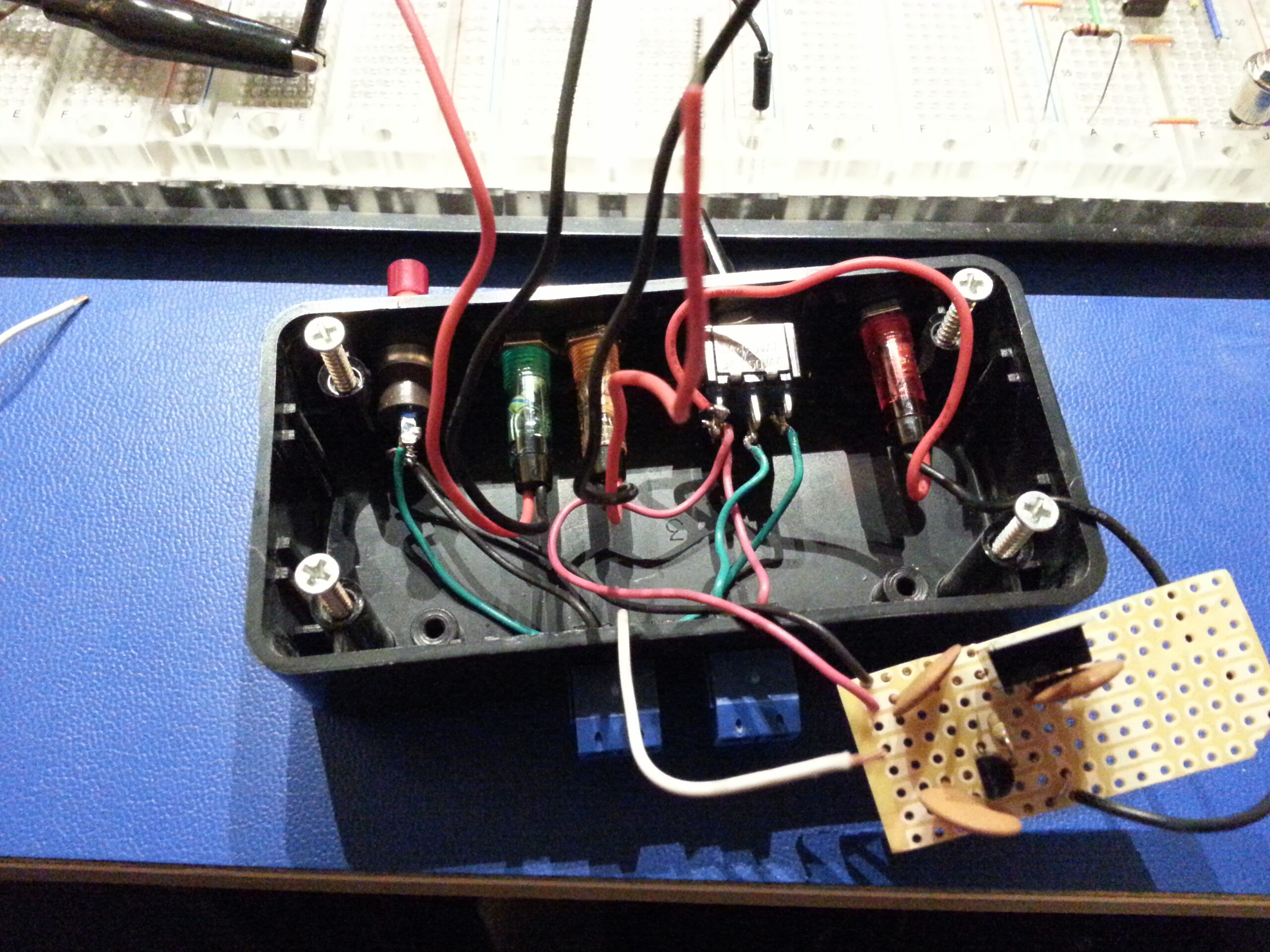
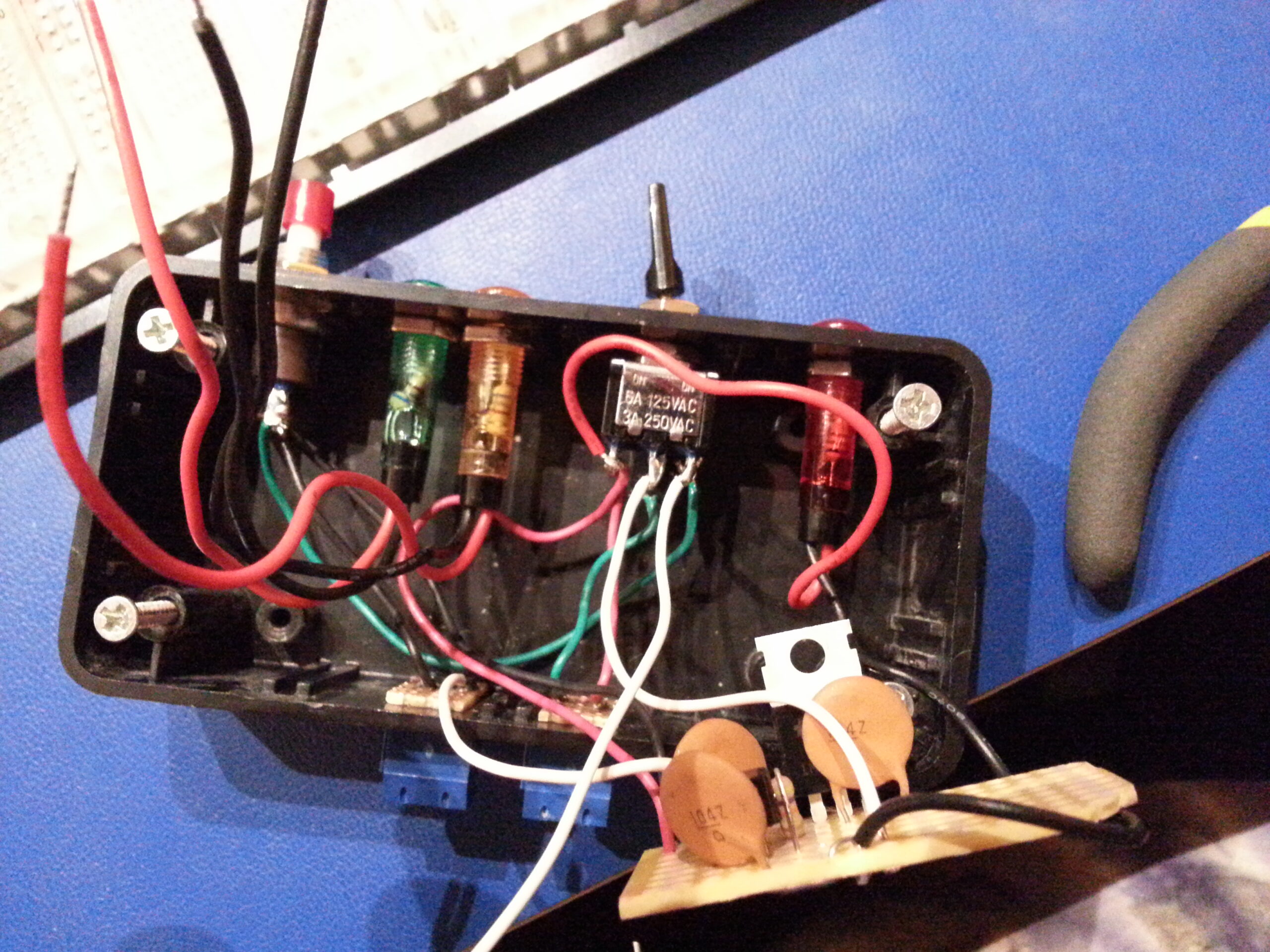
Then, once I’d put all of the parts in place I made a few measurements (idiot test) to make sure I got it right. A quick look at the box also informed me that I was going to need to make a notch somewhere on the board so that the wires from red LED could get to the other side. The simplest solution to that was to knock off a corner of the board.
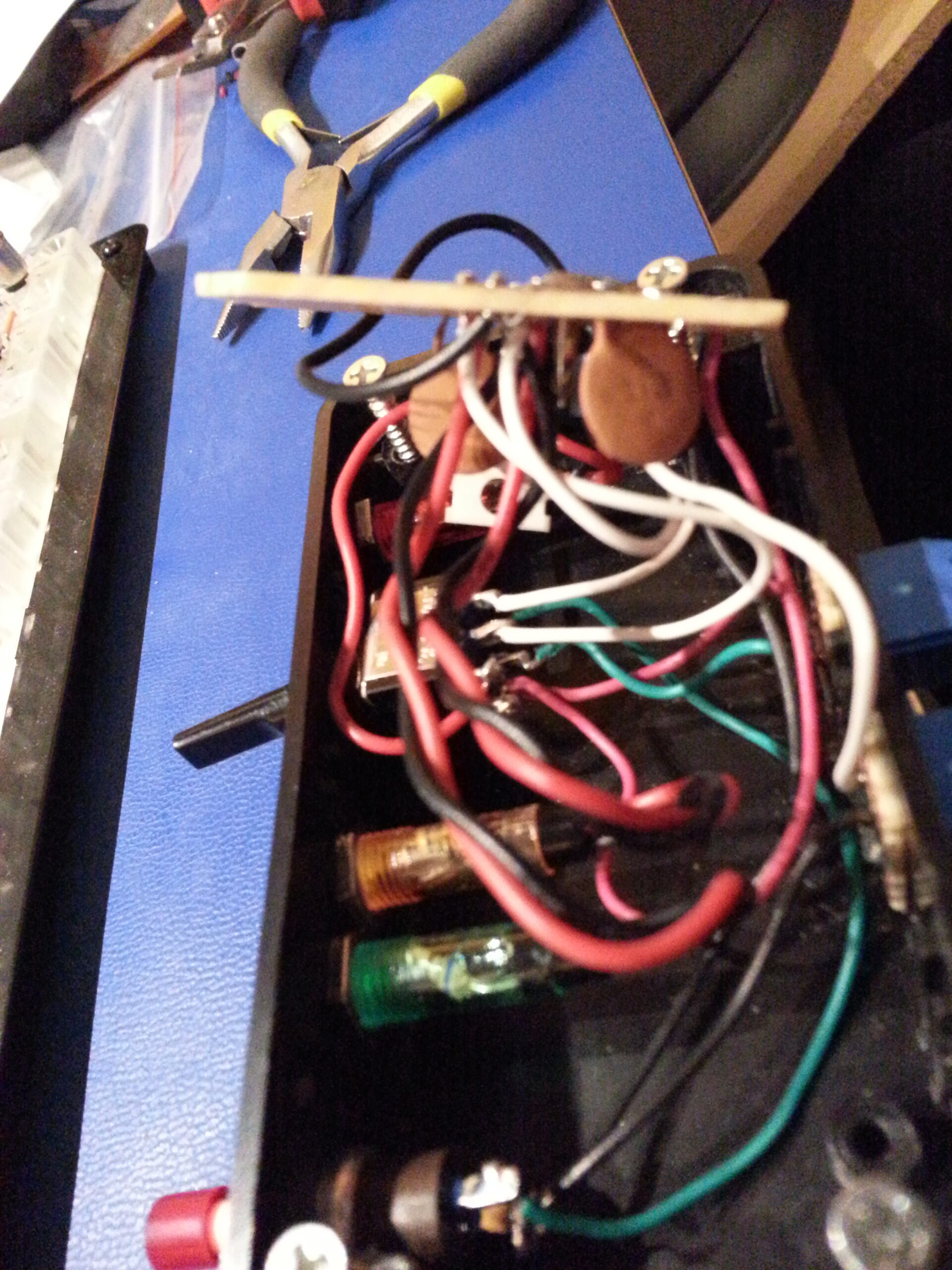
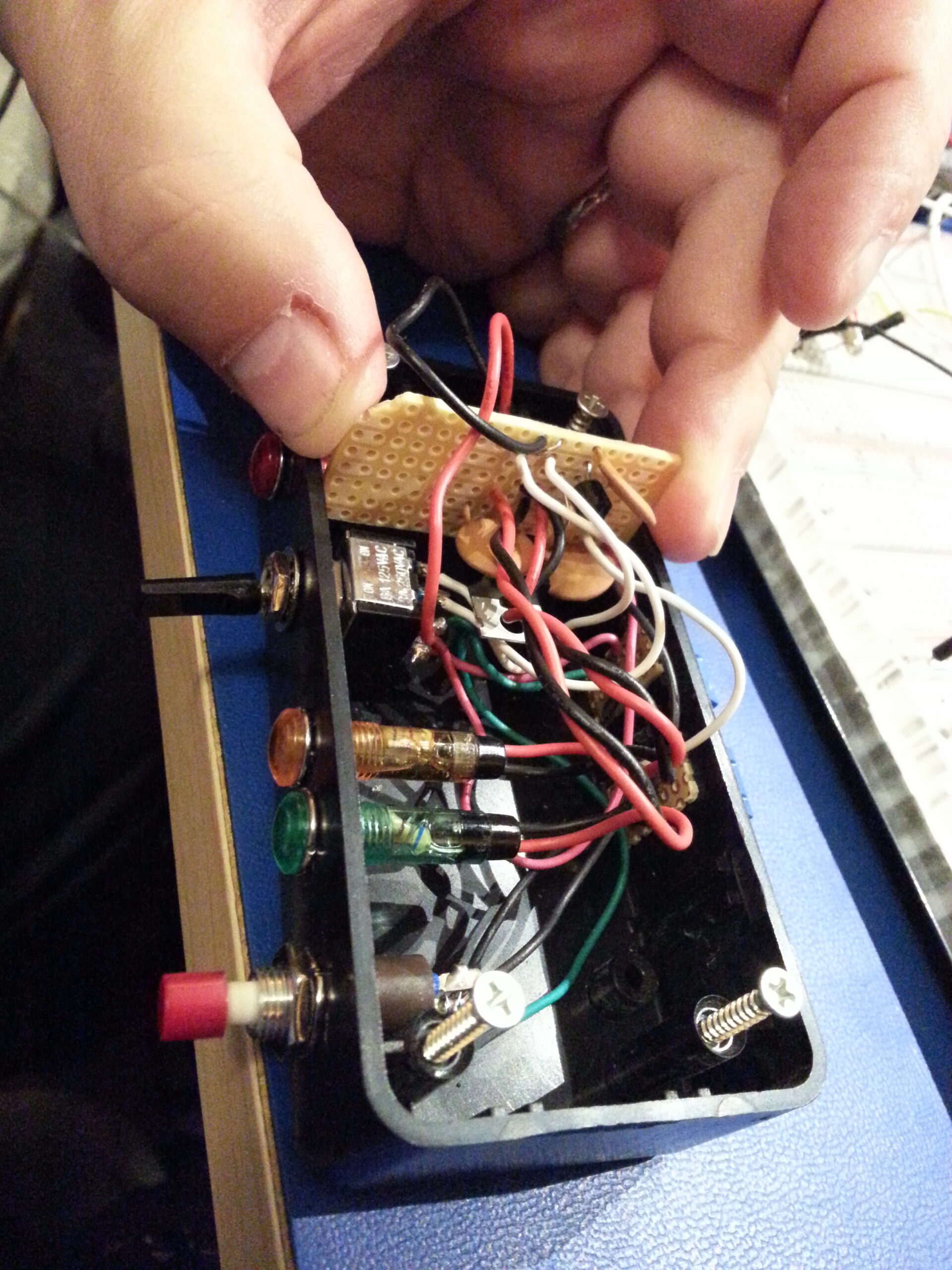
Finally I connected everything together and “stuffed” it into the box. I say “stuffed” because, well, it’s a sloppy jumble of wires going everywhere all kind-of crammed into that space. I thought about making it neater, or maybe doing a more sophisticated PCB that would eliminate much of the wiring, but in the end this was a quick-and-dirty job. As such, the extra length of the wires was needed in order to be able to assemble and disassemble the device for testing and/or changes.
If you make the wires too short then there’s no room for getting the circuit board into and out of the box without having to desolder something. The lead length also doesn’t matter too much in this case since it’s all low-voltage DC, and the heat dissipation requirements are vanishingly small – so “stuff” it is.
Make one connection at a time until everything is wired up, make a final test, then it’s stuff-in-a-box. 🙂
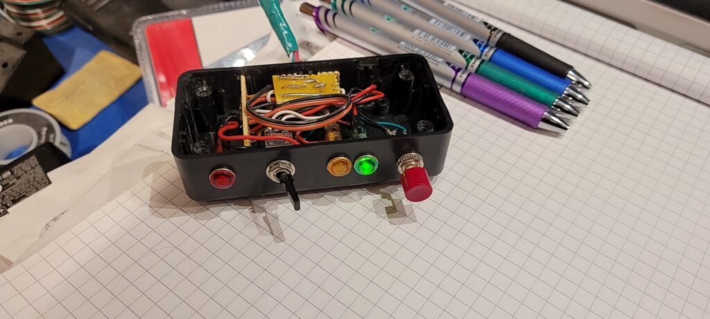
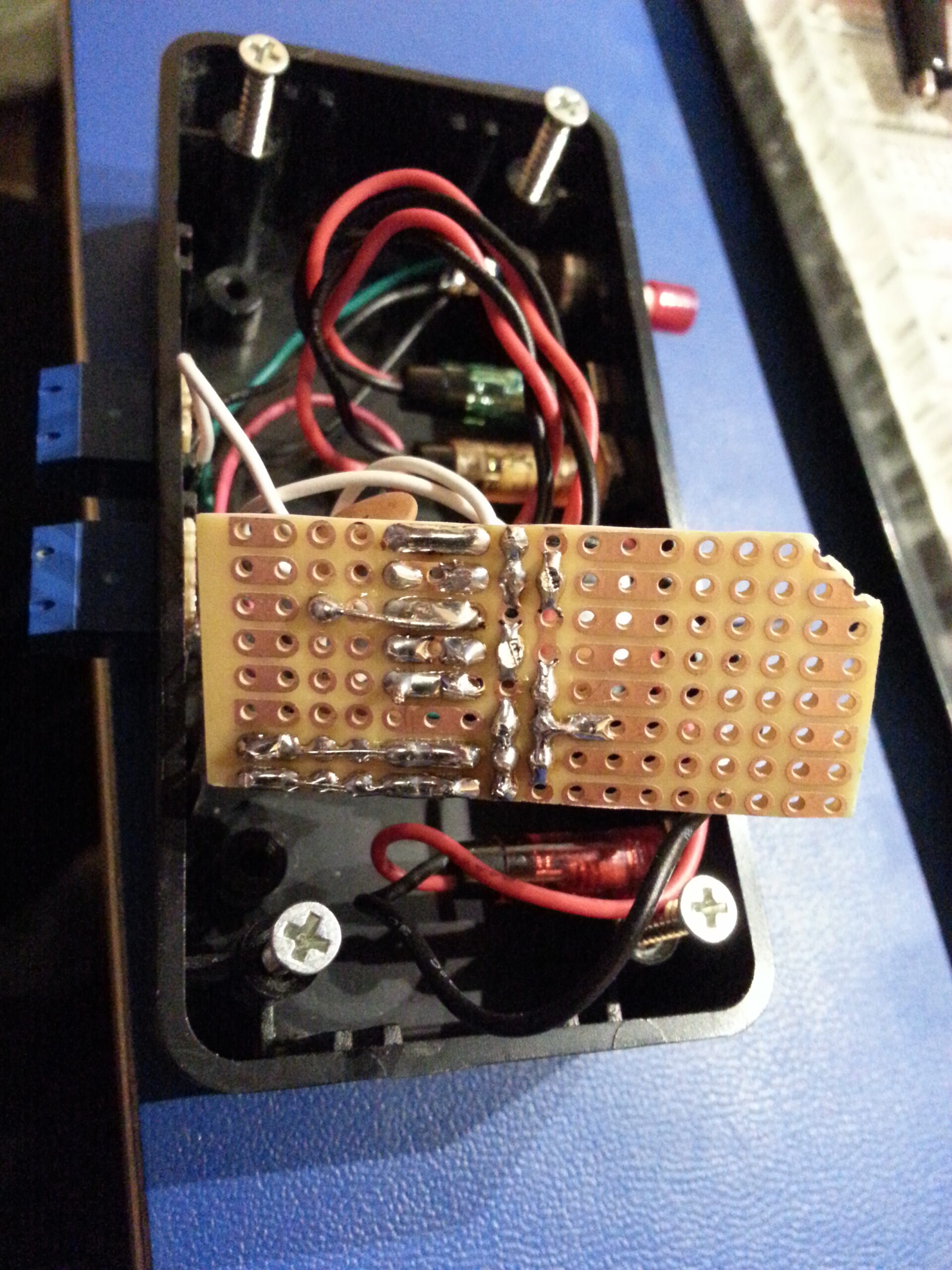
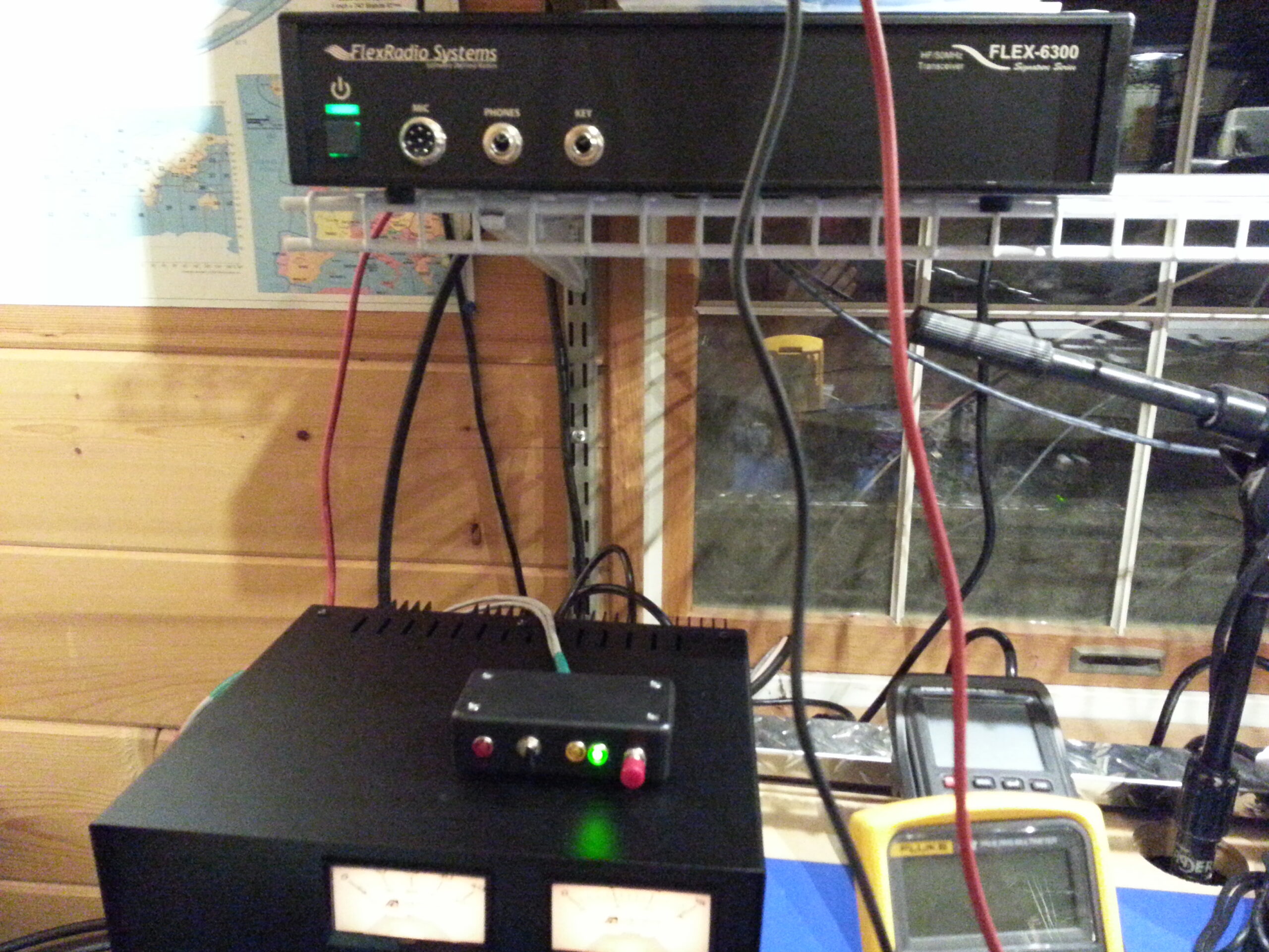
Once the lid is on and it’s up and running it’s a pretty solid and fairly professional presentation. The LEDs all work as expected, and the orientation of the toggle switch and the red “do-not-tune” light make the user interface intuitive. With the switch to the left (away from the controls) the red LED is on and the controls are locked. With the switch to the right (toward the controls) the tuner is free to tune and can be reset with the push-button.
I’ve thought about doing something more sophisticated with this… and maybe putting it in a heavier box; but ultimately it does the job, has been reliable, and there really isn’t more to do!
In future, maybe, if I built a feed-point tuner I might like to have it provide information about its’ tuning solution and even provide an analysis of the antenna… or perhaps also take commands to fine-tune the solution or act as a pre-selector … but that’s just me dreaming and NOT what this tuner does. This one is designed to be simple and reliable and it hits those marks very well.
This controller seems to hit those marks too — with just one extra blinkenlight 🙂